
High-Density Interconnect PCB Manufacturing from Prototype to Production
GemTech PCB is a China-based HDI PCB manufacturer who delivers end-to-end High-Density Interconnect (HDI) PCB—ranging from early engineering review and prototyping to advanced volume production. We support your PCB projects with precision microvias, fine-line routing, DFM and PCB manufacturing solutions.
Precision Microvias · Fine-Line Routing · DFM Support
Prototyping values selected
Our HDI PCB manufacturing capabilities satisfy demanding technical HDI PCB specifications from quick-turn prototypes to complex mass production. We specialize in laser-drilled microvias, advanced fine-line HDI PCB routing, and precise sequential lamination stack-ups that strictly comply with international reliability standards.
Swipe each table horizontally to compare Prototyping and Mass Production.
1. Stack-Up & Materials
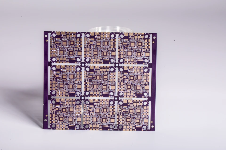
Multi-layer HDI stack-up with sequential lamination and various materials.
Parameter
Prototyping
Mass Production
Maximum Layer Count
28 layers
18 layers
Finished Board Thickness
0.15–3 mm
0.2–2.4 mm
Dielectric Material Thickness
0.025 mm (25 μm)
0.025 mm (25 μm)
Inner-Layer Copper Thickness
0.25–4 oz
0.25–3 oz
Outer-Layer Copper Thickness
0.25–4 oz
0.25–3 oz
Supported Laminate Materials
FR4, BT, high-speed laminates
FR4, BT, high-speed laminates
2. Microvia & Drilling
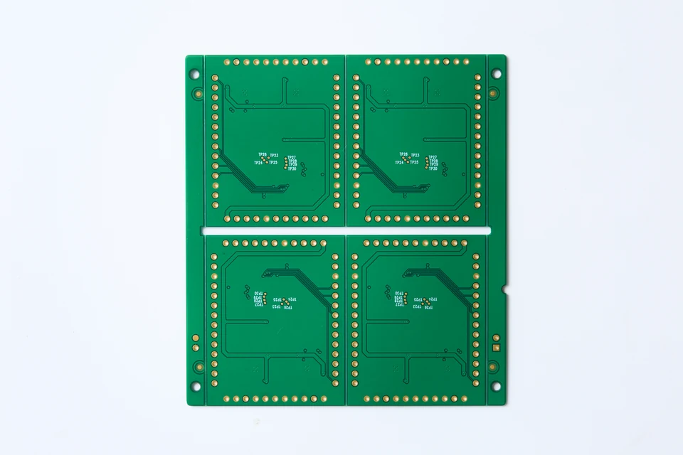
Laser-drilled blind vias, buried vias, stacked and staggered microvias.
Parameter
Prototyping
Mass Production
Minimum Blind Via Drill Diameter
0.05 mm
0.06 mm
Minimum Buried Via Drill Diameter
0.10 mm
0.12 mm
Minimum Through-Hole Drill Diameter
0.10 mm
0.12 mm
Laser Via Aspect Ratio
1:1
0.8:1
Maximum PTH Aspect Ratio
12:1
10:1
PTH Hole Diameter Tolerance
±0.035 mm
±0.05 mm
3. Fine-Line & BGA
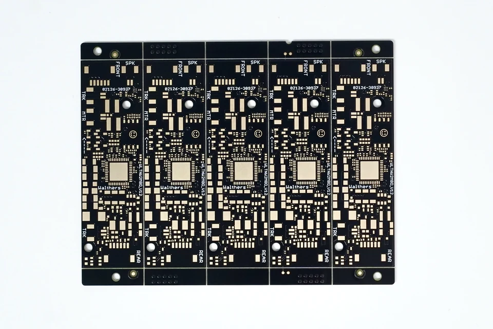
Fine-line patterning with tight line width and spacing and fine-pitch BGA.
Parameter
Prototyping
Mass Production
Inner-Layer Trace Width / Spacing
30 / 30 μm
35 / 35 μm
Outer-Layer Trace Width / Spacing
30 / 30 μm
35 / 35 μm
Minimum BGA Pad Diameter
0.13 mm
0.15 mm
Minimum BGA Pitch
0.25 mm
0.30 mm
Controlled Impedance Tolerance
±5%
±8%
Gold Finger Spacing
0.10 mm
0.10 mm
4. Via-in-Pad & Special Processes
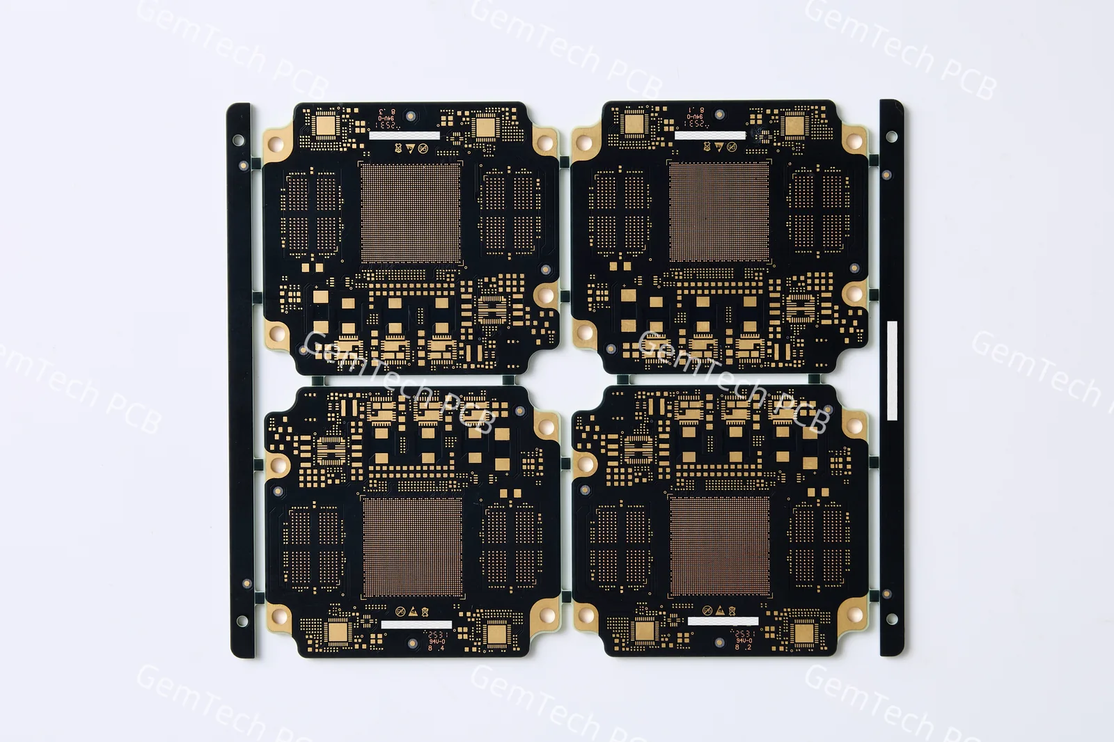
Via-in-pad, filled vias and advanced HDI processes.
Parameter
Prototyping
Mass Production
Minimum Resin-Plugged Hole Diameter
0.15 mm
0.15 mm
Maximum Resin Plugging Aspect Ratio
16:1
12:1
Minimum Solder-Mask-Plugged Hole
0.125 mm
0.15 mm
Maximum Solder Mask Plugging Ratio
10:1
8:1
Special Processes
POFV, half-hole, controlled-depth drilling
POFV, half-hole, controlled-depth drilling
5. Quality & Surface Finish
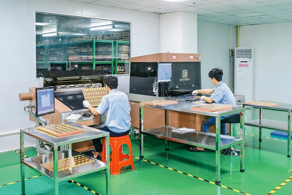
Multiple surface finishes and inspection and test reports.
Parameter
Prototyping
Mass Production
Electrical Testing
YES
YES
Microsection
YES
YES
Time Domain Reflectometry Test
YES
YES
Interconnect Stress Testing
YES
YES
IPC-6012 Class 1, 2, 3 and ES
YES
YES
View complete HDI data sheet — 55 parameters
Stack-Up & Materials
Maximum Layer Count
Prototyping: 28 | Mass Production: 18
Finished Board Thickness / Range
Prototyping: 0.15–3 mm | Mass Production: 0.2–2.4 mm
Dielectric Material Thickness
Prototyping: 0.025 mm (25 μm) | Mass Production: 0.025 mm (25 μm)
Thickness Tolerance (based on board thickness)
Prototyping: ±10% | Mass Production: Pending confirmation
Inner-Layer Copper Thickness
Prototyping: 0.25–4 oz | Mass Production: 0.25–3 oz
Outer-Layer Copper Thickness
Prototyping: 0.25–4 oz | Mass Production: 0.25–3 oz
Supported Laminate Materials
Prototyping: FR4、BT、高速(低损耗、超低损耗) | Mass Production: FR4、BT、高速(低损耗、超低损耗)
Material Type / Supported Laminate Families
Prototyping: FR4、BT、高速(低损耗、超低损耗) | Mass Production: FR4、BT、高速(低损耗、超低损耗)
Microvia & Drilling
Minimum Blind Via Drill Diameter
Prototyping: 0.05 | Mass Production: 0.06
Minimum Buried Via Drill Diameter
Prototyping: 0.1 | Mass Production: 0.12
Minimum Through-Hole Drill Diameter
Prototyping: 0.1 | Mass Production: 0.12
Laser Via Aspect Ratio
Prototyping: 1:1 | Mass Production: 0.8:1
Maximum Plated Through-Hole Aspect Ratio
Prototyping: 12:1 | Mass Production: 10:1
Blind Vias
Prototyping: 0.05 | Mass Production: 0.06
Buried Vias
Prototyping: 0.1 | Mass Production: 0.15
PTH Hole Diameter Tolerance
Prototyping: ±0.035 | Mass Production: ±0.05
NPTH Hole Diameter Tolerance
Prototyping: ±0.025 | Mass Production: ±0.03
Backdrill Through-Hole Diameter
Prototyping: 0.15 | Mass Production: 0.2
Backdrill Hole Diameter
Prototyping: D+0.15 | Mass Production: D+0.15
Backdrill Depth Tolerance
Prototyping: ±0.05 | Mass Production: ±0.075
Residual Backdrill Stub
Prototyping: 0.05-0.20 | Mass Production: 0.05-0.20
Fine-Line & BGA
Minimum BGA Pad Diameter
Prototyping: 0.13 | Mass Production: 0.15
Minimum BGA Pitch
Prototyping: 0.25 | Mass Production: 0.3
Gold Finger Width
Prototyping: 0.1 | Mass Production: 0.13
Gold Finger Spacing
Prototyping: 0.1 | Mass Production: 0.1
Minimum Trace Width / Spacing — Inner Layer
Prototyping: 30 / 30 μm | Mass Production: 35 / 35 μm
Minimum Trace Width / Spacing — Outer Layer
Prototyping: 30 / 30 μm | Mass Production: 35 / 35 μm
Controlled Impedance Tolerance
Prototyping: ±5% | Mass Production: ±8%
Via-in-Pad & Surface Finish
Minimum Dam / Web Size — SMT
Prototyping: 0.05 | Mass Production: 0.06
Minimum Dam / Web Size — BGA
Prototyping: 0.05 | Mass Production: 0.06
Minimum Resin-Plugged Hole Diameter
Prototyping: 0.15 | Mass Production: 0.15
Maximum Resin Plugging Aspect Ratio
Prototyping: 16:1 | Mass Production: 12:1
Minimum Solder-Mask-Plugged Hole Diameter
Prototyping: 0.125 | Mass Production: 0.15
Maximum Solder Mask Plugging Aspect Ratio
Prototyping: 10:1 | Mass Production: 8:1
Surface Finishes Available
Prototyping: OSP、ENIG、OSP+ENIG(选择性)、LF HAL、ENEPIG、镀金 | 化金、OSP、化金+OSP、电镀硬金、镍钯金、镍钯金+OSP | Mass Production: OSP、ENIG、OSP+ENIG(选择性)、LF HAL、ENEPIG、镀金 | 化金、OSP、化金+OSP、电镀硬金、镍钯金、镍钯金+OSP
Special Processes
Prototyping: 侧壁金属化、半孔、沉孔、深度控制钻、POFV | 控深钻、沉头孔、金手指、POFV、侧边金属包边、半孔、Cavity等 | Mass Production: 侧壁金属化、半孔、沉孔、深度控制钻、POFV | 控深钻、沉头孔、金手指、POFV、侧边金属包边、半孔、Cavity等
Quality & Testing
Electrical Testing
Prototyping: YES | Mass Production: YES
Microsection
Prototyping: YES | Mass Production: YES
Solderability
Prototyping: YES | Mass Production: YES
Ionic Contamination
Prototyping: YES | Mass Production: YES
Time Domain Reflectometry (TDR) Test
Prototyping: YES | Mass Production: YES
First Article Inspection (FAI)
Prototyping: YES | Mass Production: YES
Hi-Pot Test
Prototyping: YES | Mass Production: YES
Interconnect Stress Testing (IST)
Prototyping: YES | Mass Production: YES
D Coupon / Test Coupon
Prototyping: YES | Mass Production: YES
IPC-6012 / Class 1, 2, 3 and ES
Prototyping: YES | Mass Production: YES
IPC-6013 / Class 1, 2 and 3
Prototyping: YES | Mass Production: YES
MIL-PRF-55110 (selected materials)
Prototyping: YES | Mass Production: YES
UL Recognition / UL 94V-0
Prototyping: YES | Mass Production: YES
Other Parameters
Panel Size / Maximum Shipped Panel Size
Prototyping: 500×280 | Mass Production: 500×280
Board Warpage
Prototyping: ≤0.30% | Mass Production: ≤0.5%
CNC Routing Tolerance
Prototyping: ±0.05 | Mass Production: ±0.075
Countersink
Prototyping: Listed as 沉孔 in special processes; confirm terminology / Listed as 沉头孔 in special processes; confirm terminology | Mass Production: Listed as 沉孔 in special processes; confirm terminology / Listed as 沉头孔 in special processes; confirm terminology
Edge Castellation / Half-Hole Diameter
Prototyping: Min 0.35 | Mass Production: Min 0.4
Edge Plating / Sidewall Metallization
Prototyping: Sidewall metallization listed in special processes / Sidewall metallization / side-edge metal wrapping listed in special processes | Mass Production: Sidewall metallization listed in special processes / Sidewall metallization / side-edge metal wrapping listed in special processes
Values are shown as Prototyping / Mass Production. Technical specifications vary by material, stack-up, copper thickness and design requirements. Final manufacturability is subject to engineering review.
Megtron 6, RO4350B and FR408HR are fully qualified and in mass production on our HDI production line, with stable lamination process and consistent yield above 97%.
GemTech PCB offers prototyping HDI circuit boards with fine-pitch BGA, high-speed RF and miniaturized industrial applications, including mmWave radar, portable medical electronics and high-density FPGA boards. At GemTech, you get a fully functional, testable HDI prototype on a predictable timeline and budget.
Also, the HDI PCB manufacturing solution is for critical applications across ADAS, EV electronics, medical device manufacturing, and 5G communications.
Automotive HDI PCB
ADAS PCB and EV electronics PCB designs with dense signal routing, compact control circuits, and integrated sensing functions.
Medical HDI PCB
Compact medical PCB designs for portable monitoring, diagnostics, and medical electronics. Key considerations include traceability, test access, and manufacturing consistency.
Telecommunications HDI PCB
5G PCB, high-speed PCB, and RF PCB designs requiring dense interconnections, controlled impedance, and application-specific materials.
Aerospace HDI PCB
High-reliability HDI PCB designs for space- and weight-constrained electronics. Defense PCB projects require manufacturing controls, traceability, and qualification matched to the program.
Consumer Electronics HDI PCB
Compact electronics PCB and fine-pitch BGA PCB designs that integrate more components within limited board space.
Semiconductor Test PCB
Test interface PCB and high-density test board designs requiring dense device connections, precise routing, and signal integrity control.
HDI & RF Applications
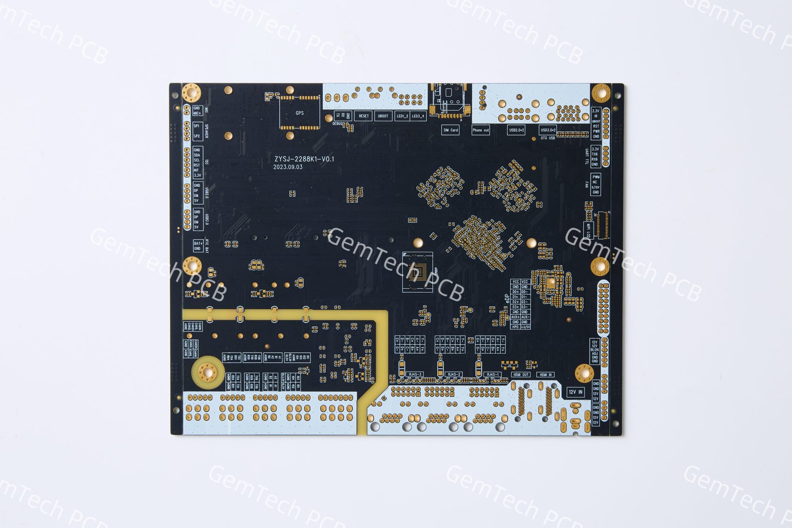
AI Computing Board · 40612
14-Layer | 6-N-6 HDI
High-density interconnections for AI hardware, deep learning accelerators, and FPGA-based computing.
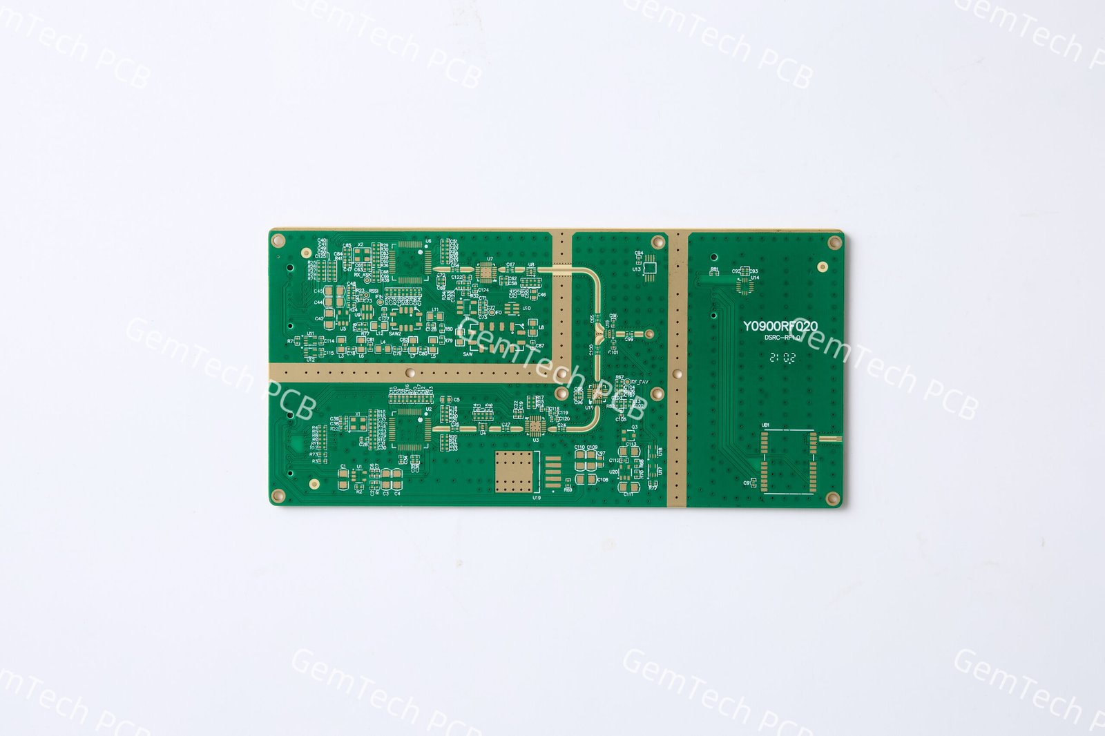
Drone Mainboard · 43147
8-Layer | 2-N-2 HDI
Compact integration for flight control and RF image transmission in drone electronics.
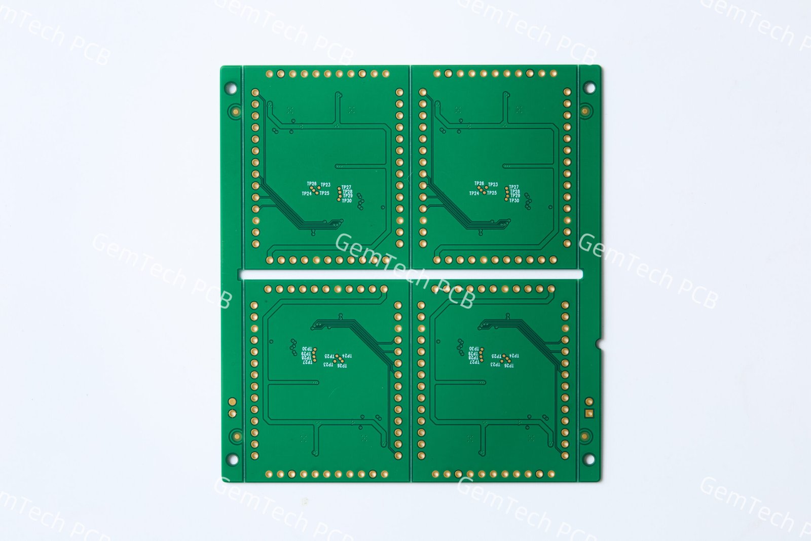
Industrial Controller · 32768
6-Layer | 1-N-1 HDI
Compact multilayer construction for industrial automation and embedded control systems.
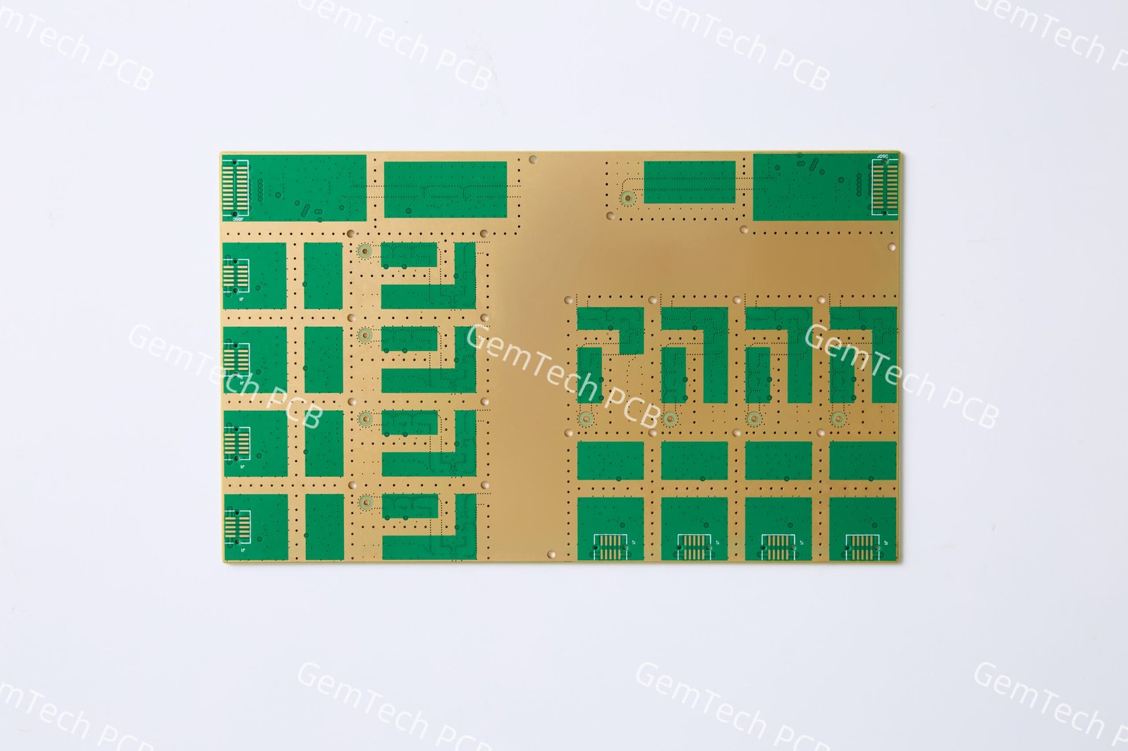
Phased Array RF Antenna Board
High-Frequency Stackup
Dense antenna array routing for mmWave radar and 5G communications.
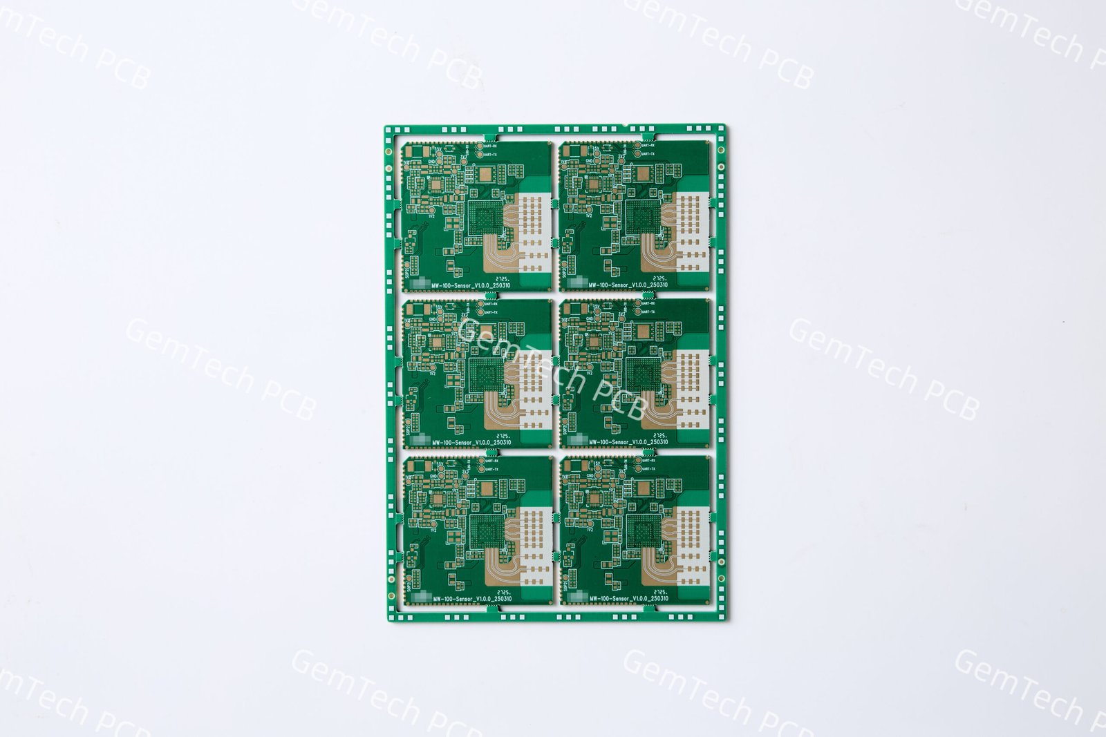
Rogers + FR4 Industrial Sensor
Hybrid Stackup
Compact industrial sensors and portable medical electronics.
Images are representative. Project details and case study links are pending confirmation.
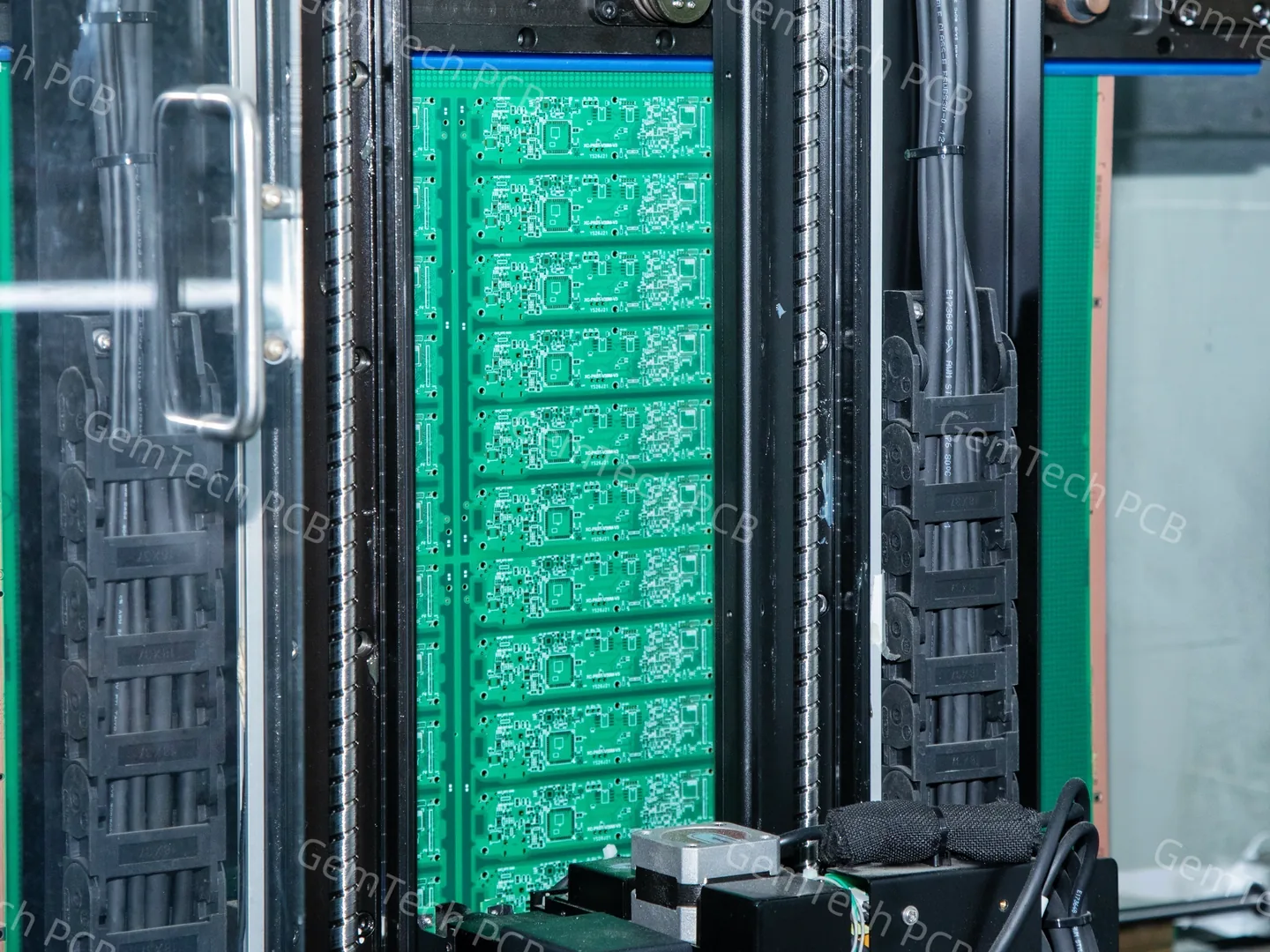
Whether supporting rapid NPI prototyping or seamless volume mass production, we combine state-of-the-art UV/CO2 laser drilling and automated optical registration lines to fulfil precise hole structures engineered for extreme density and long-term reliability.
Equipment & Process: High-precision UV/CO2 laser drill systems for precise layer-stop control.
Delivery & Capabilities: Custom laser-drilled blind via builds and dense HDI blind via stack-ups ship with zero inner-layer damage on every blind via PCB order.
Equipment & Process: Sub-stack lamination presses with 100% resin-plugging lines.
Delivery & Capabilities: Internal routing channels remain completely sealed through specialized buried via PCB processing, yielding enclosed HDI buried vias and heavy-duty multilayer PCB vias.
Equipment & Process: Advanced pulse-plating copper filling for void-free vertical microvia stacks.
Delivery & Capabilities: Solid copper stacked microvias eliminate internal voiding in high-aspect-ratio stacked microvia PCB runs, unlocking extreme BGA routing for high-density interconnect PCB designs.
Equipment & Process: High-accuracy laser registration tooling with strict pitch controls.
Delivery & Capabilities: Spatially offset staggered microvias reduce Z-axis thermal expansion stress on the staggered microvia PCB, directly guaranteeing maximum microvia reliability.
Equipment & Process: Vacuum resin-plugging equipment, thermal curing ovens, and ceramic planarization systems for POFV (Plated-Over-Via-in-Pad).
Delivery & Capabilities: For sub-0.4mm BGA layouts, flat copper-capped via-in-pad HDI PCB surfaces eliminate solder wicking without compromising pad coplanarity.
Quality Checks Defined by the Specification
Our HDI PCB quality control complies strictly with the following standards: IPC-2226 microvia design standards and IPC-6012 Class 3 performance requirements.
• Validation & Testing: IST Stress Testing | CAF Resistance Screening | Thermal Cycling
• Factory Certifications: IATF 16949 (Automotive)
Support from Prototype Through Repeat Builds
Share your prototype quantity, forecast demand and target schedule. We can review the appropriate production route and the controls needed to maintain the agreed requirements across repeat orders, subject to actual production capability.

Our manufacturing process is organized around the agreed board construction, material requirements and quality plan. This section should introduce the facility responsible for your order, the HDI processes performed there, and any specialist operations handled by qualified partners.
Explore Manufacturing Facilities →Technical considerations and layout recommendations for RF PCB engineering
What are the key DFM layout guidelines for high-frequency RF PCBs?
High-frequency RF PCB layout requires strict control over controlled-impedance trace geometries, ground stitching via spacing (< λ/10), and layer transitions to minimize insertion loss and radiation. Ensure solid, uninterrupted reference ground planes directly underneath RF traces and use curved corners instead of 90-degree corners to avoid impedance discontinuities.
How do you select materials for RF PCBs, and when should you use hybrid stackups?
Material selection is governed by operating frequency, allowable dissipation factor (Df), and thermal demands. Hybrid stackups such as Rogers + FR-4 balance high-frequency performance with overall board cost by placing specialized substrates on RF layers and FR-4 cores for power, ground and structural rigidity.
What capabilities should you verify when choosing an RF PCB manufacturer?
Evaluate impedance verification, backdrilling precision, hybrid lamination experience, PTFE hole-wall preparation, low-loss surface finishes and applicable certifications. Confirm whether TDR coupon testing and IPC-6018 Class 3 / IATF 16949 compliance apply to your project.
Why do RF simulation results differ from fabricated board performance?
Fabrication tolerances, batch-to-batch material variation and missing parasitic details can shift insertion loss and impedance from a nominal simulation. Include trace width, copper roughness, lamination offsets, connector launch and via geometry in the engineering review.
Tell us about your board type, key specifications and production target. The team can follow up to clarify technical details and next steps.
National High-tech Enterprise
Company credential — verify current certificate
Specialized & Innovative SME
Company credential — verify current status
ISO 9001:2015
Quality management system
IATF 16949:2016
Automotive quality management
ISO 14001:2015
Environmental management system
UL / CQC
UL file E470791 and CQC — verify scope
Please confirm the validity, issuing entity and applicable scope of all certifications before publishing certificate marks or making compliance claims.
Project enquiry
Fields marked * are required.
This enquiry panel is ready to connect to your WordPress form handler.