

GEMTECH PCB
A PCB DFM review, also called a PCB design for manufacturing review, checks whether design files, dimension definitions, and manufacturing conditions refer to the same board and revision. If records conflict, raise a specific engineering question so the designer can confirm the intent and approved value. Update every affected file with that approved result before releasing the manufacturing package.
This article is for multilayer bare-board projects. It explains which records to check before manufacturing, how to distinguish objects that are easy to confuse, and how to close engineering replies into one approved revision. Each process decision still depends on the current stack-up, materials, copper thickness, hole types, and applicable process. For the fabrication sequence, see the multilayer PCB manufacturing process guide.
DRC (design rule checking) checks a layout against the rules set in the design files. If the applicable manufacturing conditions have been confirmed, requirements for trace width, spacing, and annular rings can be added to the rule set. A pass means only that the layout meets this rule set. It does not mean that every file in the manufacturing package is aligned or that the rules apply to the materials and process for this board.
A DFM (design for manufacturing) review considers the specific board and its applicable manufacturing conditions. It compares design data, manufacturing data, and process requirements item by item. Published minimum values may depend on copper thickness, hole type, layer, or other conditions. Confirm that those conditions match this board before using a value as a design requirement.
A review record can group findings into three types:
Do not infer the effective revision from a filename or date alone. Link each key requirement to the layer, file, or note that verifies it. If a requirement cannot be matched, mark it as pending confirmation.
Numbers in the same project may describe design values, production values, or finished-board acceptance values. If the layer, process stage, or unit is not clear, do not compare two minimum values as if they show a nonconformance.
Design trace width, the production copper pattern, and measurements on a finished board describe different things. State the layer and location, whether the value applies to the design or finished-board stage, the copper-thickness basis, and the acceptance condition. Copper thickness, plating, and etching affect the usable trace width and spacing range. Do not apply a published minimum from different conditions to this board.
An annular ring is the copper left around a connected pad hole. Hole-to-copper clearance is the gap between a hole and an unconnected copper feature. For concentric circular pad and hole geometry, the nominal ring width is half the difference between the pad diameter and hole diameter. This is a nominal value for concentric geometry, not the minimum remaining ring after drill offset. Before using the value, confirm whether the hole-size field means the production drill diameter or the finished hole diameter. Drill offset can make the remaining copper ring narrower in some areas.
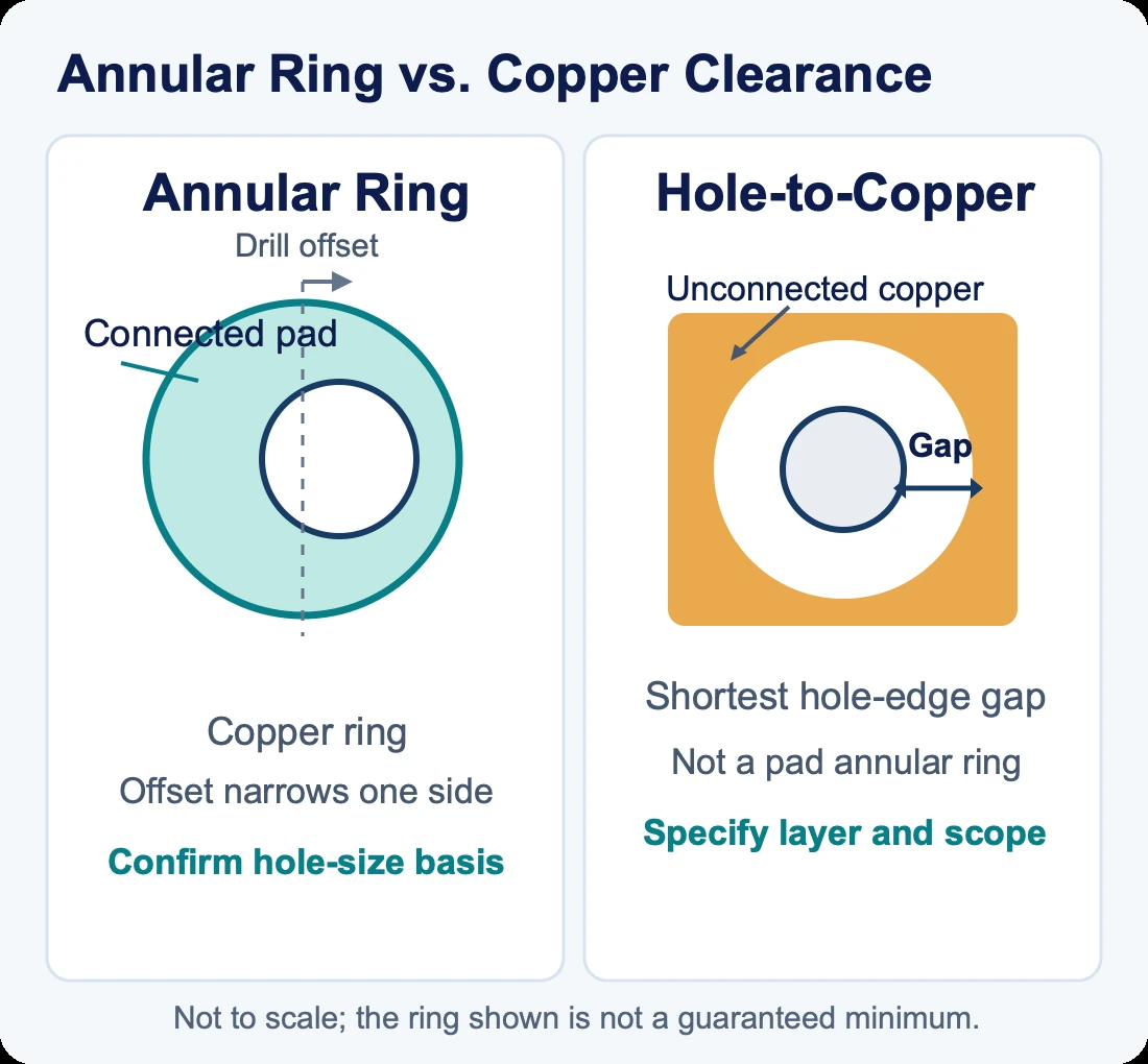
Figure 1. Top view of an annular ring and hole-to-copper clearance. The illustration is not to scale. Confirm the hole-size basis in the manufacturing data.
Do not combine annular ring and hole-to-copper clearance into one spacing requirement. In an engineering question, identify the connected pad for the hole, nearby unconnected copper, applicable layer, and hole location. A larger pad may widen the annular ring but can reduce the clearance to unconnected copper.
For a plated hole, finished hole diameter and production drill diameter are different fields. Design data should state the finished hole size, unit, tolerance, and hole type. Label PTH (plated through-hole) and NPTH (non-plated through-hole) separately. For blind and buried vias, also state the connected layer range. The fabricator can then check the production drill data against those requirements.

Figure 2. Mechanical PCB drilling equipment on the factory floor.
Solder-mask openings must align with the pad type and mask registration conditions. A larger opening can help preserve exposed pad copper when the mask is misaligned, but it narrows the solder-mask bridge between adjacent openings. Check both exposed pad area and the remaining mask bridge. If the fabricator may adjust the openings, state the allowed adjustment range and approval method in the fabrication notes. Carry the approved result into the new revision.
Copper-to-edge clearance must match the finished outline and layer. First identify whether the outline data refers to an individual board or a panel. Then check the requirement for each copper layer against the named boundary. A routed edge, V-score line, and process edge are different boundaries. Do not use one undefined "board edge" for all three.
Confirm the material, finished board thickness, copper thickness for each layer, and dielectric thickness against the same stack-up revision. Starting copper foil thickness does not replace the finished outer-layer copper-thickness requirement. If copper thickness, layer count, or material changes, recheck the related trace constraints, layer connections, and target impedance.
Controlled impedance must specify the trace layer, reference layer, trace width, differential spacing, material, and dielectric thickness, along with the target value and allowed tolerance. If the stack-up, impedance table, or drawing disagrees on layer count, board thickness, or trace layer, identify the effective revision first. Do not combine values from separate files into a manufacturing requirement.
For example, an anonymized set of project records lists a nominal finished-board thickness of 1.6 mm with both ±10% and ±0.10 mm tolerances. At 1.6 mm, ±10% equals ±0.16 mm and gives an acceptance range of 1.44 to 1.76 mm. A ±0.10 mm tolerance gives a range of 1.50 to 1.70 mm. The ranges are not equivalent. Use the same range approved by the designer in the fabrication drawing, stack-up, and inspection requirements.
The phrase "Please confirm" does not tell the other person what to review. An engineering question should let the designer and fabricator decide using the same location and data. Use this sequence:
For example, if the fabrication drawing and stack-up table use different board-thickness tolerances, ask which acceptance range applies and whether both files need updating. Asking for a specific decision is more useful than writing only "Please confirm the tolerance."

Figure 3. Four-step DFM review path from checking manufacturing data through approval and revision release.
Engineering approvals should not stay only in email or chat. Enter approved values in the fabrication drawing, stack-up, drill data, copper layers, solder-mask data, and related inspection requirements. If a file does not need an update, list the revision that remains in effect on the release checklist.
Before releasing the manufacturing package, check each item:
If a later change affects holes, traces, solder mask, stack-up, or outline, review each affected item again before releasing a new revision. For the layer sequence and material relationships of a multilayer board, see the multilayer PCB stack-up guide. Use the stack-up approved for this board.
For information about multilayer bare-board manufacturing, see the multilayer PCB manufacturing page. When the board structure and manufacturing data are ready, submit the project files through the bare-board fabrication quote form. For process selection by exposed-copper use, see the PCB surface finish selection guide.


