
An HDI PCB, or high-density interconnect printed circuit board, uses microvias with short layer spans and smaller connection pads. It also pairs these structures with fine-line geometry to create more routing space for dense components. When choosing HDI, first check whether component pins can fan out and which layers the signals must reach. Then compare via structures and the added manufacturing steps. Two boards with the same layer count can still use different connection structures.
The first difference is the space used by each local connection. A multilayer PCB has several copper layers. Higher local connection density also requires vias, pads, and traces to fit in limited space and connect to the needed copper layers. For this reason, microvias and buildup structures can limit a layer transition to the span the connection needs instead of using a via that passes through the entire board.
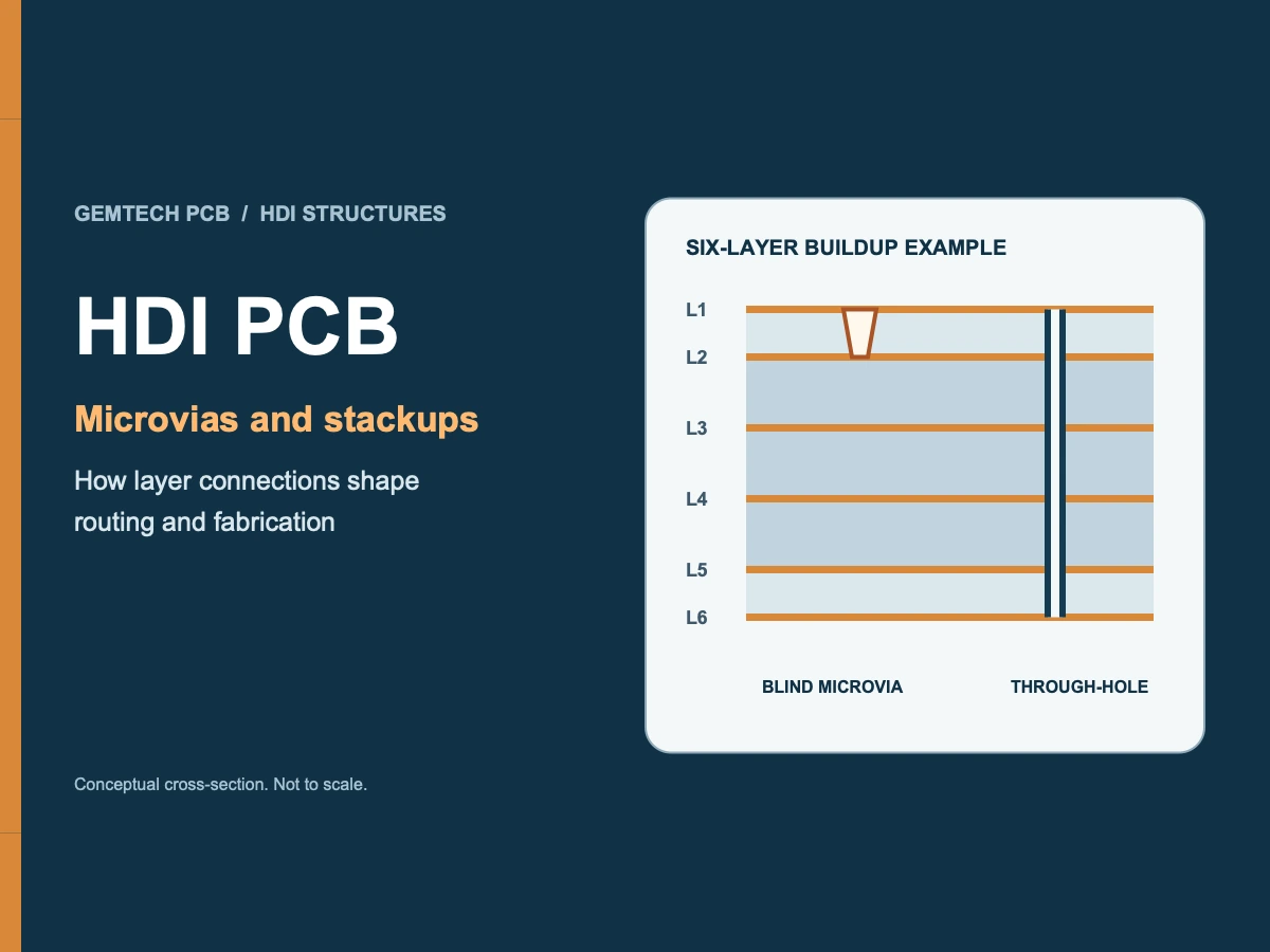
For example, on a six-layer board, a signal that only needs to connect L1 to L2 can use either a through via or an L1 to L2 blind microvia. The through via still passes through L1 to L6, so routing on later layers must avoid that via and its required pads or clearances. The blind microvia ends at L2 and does not pass through L3 to L6. This compares two via structures for the same connection task, not boards with different total layer counts.
A via passing through a layer is not necessarily electrically connected to that layer's copper. Connected layers use pads. Nonconnected copper layers need clearance around the via. To assess the space it uses, check the opening and pads as well as the copper layers it crosses. The visible hole diameter alone does not show the limits on internal routing.
For a general view of how copper layers, cores, and prepreg form a multilayer stackup, see the multilayer PCB structure guide. HDI adds denser layer connections to these base structures. The choice still needs to preserve the required reference planes, dielectric thickness, and electrical connections.
Compare blind vias, microvias, or other stackup options when the component pad pitch and through-via pads leave no route for the required trace width and spacing. Fanout carries a component package pad to a point where routing can continue. It depends on the package pad array and the via and trace geometry.
Device fanout, pad pitch, and stackup jointly determine via selection. A BGA package can be evaluated with both through-via and blind-via options. If there is room to route between pads for through vias and an escape path remains for pads in the inner rows, a conventional structure may work. If vias and pads block connections to the inner rows, shorter layer spans or smaller microvias may free routing space. A BGA alone does not mean the whole board needs one HDI structure.
When evaluating an HDI PCB, compare the layer count and manufacturing steps together. Adding conventional signal layers may help routing, but it does not reduce the space occupied by existing through vias. Buildup microvias may free routing channels, but they change the sequence for hole formation, metallization, and lamination. The selected structure must complete the required connections and match the project's manufacturing requirements.
Through vias, blind vias, and buried vias are classified by their start and stop layers in the finished board and by whether the hole is visible from the outside. Microvias describe short-span hole structures and their formation method, so the terms can overlap. An L1 to L2 microvia can also be a blind via. The terms blind via and microvia do not describe mutually exclusive choices.

Figure 1. A conceptual six-layer cross-section showing a through via, mechanical blind via, mechanical buried via, and outer-layer blind microvia. Layer numbers show the connection spans. The microvia is drawn in a thinner outer buildup dielectric. The diagram is not to scale.
The target pad is the copper pad that receives a microvia at its bottom. The via must land accurately on that copper and form the required connection along its wall and at its bottom. To continue to deeper layers, microvias can be staggered or stacked at matching connection points. A staggered structure needs connection space on the intermediate layer. In a stacked structure, each upper via lands on the connection point below. The lower via fill and the flatness of its copper landing surface must be confirmed for the upper via design.
The layer spans of blind and buried via connections across layers can be compared pair by pair. The relevant microvia options include single, stacked, and staggered microvia structures. Both questions can arise within one stackup, but a general count of via stages cannot replace a precise via map.
Via-in-pad describes a location. It places a via inside a component pad instead of beside it, reducing the space needed by nearby routing. If that pad is also on a soldering surface, the pad surface and opening must be addressed. Moving a via to the center of a pad in the layout does not complete the design.
For an open mechanical through via inside a pad, solder may enter the hole during reflow and change the amount of solder available at the joint and the surface shape. VIPPO means via-in-pad plated over. It uses filling and copper capping to create a usable pad surface. Via filling, copper capping, and planarization have different roles. Filling treats the hole cavity. The copper cap covers the opening. Planarization reduces the local surface height difference.
The fill material and the electrical connection are separate questions. A resin-filled plated via can still conduct through its via-wall copper. A copper-filled microvia fills the hole cavity with copper. These structures have different purposes. For a stacked connection with another microvia above, the lower landing surface must work with the next via. For a via inside a component pad, the solderable surface requirements must also be specified.
Choosing between via-in-pad and VIPPO starts with the via location and soldering surface. The differences between resin filling, copper filling, and copper capping determine the required treatment. This article covers bare-board connections and surface conditions. Package pad requirements from assembly should be treated as design inputs.
HDI manufacturing tradeoffs depend on which vias the structure uses, when they are formed, and how many buildup cycles it requires. A sequential buildup process adds dielectric and copper to a core in stages, then forms the corresponding layer connections. Therefore, even with six copper layers, a through-via multilayer design and a buildup microvia design can follow different manufacturing routes.
Figure 2 uses a 1+4+1 concept to show the sequence. First make the L2 to L5 four-layer core and its core vias. Then add the dielectric and copper for L1 and L6 on both sides. Form the outer microvias and complete metallization and the outer-layer pattern. Repeat stages only if the design calls for further buildup. The 1+4+1 notation describes the layer construction, not the full manufacturing sequence, which also includes making the core.

Figure 2. A sequential buildup concept for a 1+4+1 construction. The core build, buildup, outer-layer hole formation, and metallization are shown in separate stages. Filling or copper capping depends on the selected structure.
This sequence explains why HDI should not be priced by total layer count alone. Buildup connections can add lamination, hole formation, and metallization steps. A stacked structure may also require lower-via filling. A via-in-pad structure may require filling and copper capping. These choices add specific processing steps and surface requirements. If a microvia structure reduces the number of other routing layers needed, it can also change the cost composition of the full board. Compare alternatives for the same connection task and acceptance conditions. Do not apply a fixed price multiplier.
The buildup and via processing in HDI sequential lamination are a separate topic from the general multilayer manufacturing sequence. The overall sequence of inner-layer imaging, pattern transfer, and bare-board inspection is covered in the multilayer PCB manufacturing process. Keep these topics separate so a general multilayer process list does not stand in for HDI buildup steps.
Before release, align the thickness and connection details for the same structure. Finished board thickness describes the full board. Individual dielectric thickness affects microvia depth. Whether a core thickness includes copper changes how that field should be read. These values can appear in the same stackup, but they are not interchangeable.
One local six-layer HDI project record specifies a 0.6 mm finished board thickness and a 0.17 mm copper-clad core. The first is a requirement for the finished board. The second describes a specific core component that includes copper. The 0.17 mm value is not the pure dielectric thickness inside the core. The 0.6 mm board thickness is not the drilling depth for an outer-layer microvia.
For each via type, confirm the depth and diameter definitions for via aspect ratio. A mechanical through via spans a different depth from a local outer-layer microvia. Drill diameter and finished hole diameter are also different inputs. After mapping these fields, check the manufacturing package in this order.
Use the PCB DFM checklist before manufacturing to check file completeness and approval status. For a specific bare-board review, see HDI bare-board manufacturing and review. Submit the stackup and via requirements through the HDI project quote request.


