
GEMTECH PCB · TECHNICAL GUIDE
A multi-layer printed circuit board has three or more conductive copper layers laminated into one board, with insulating material between them. If you are comparing 4-, 6-, and 8-layer designs, copper-layer count is only a starting point. You also need to see which layers route signals or serve as reference planes and how the materials are arranged between those layers.
A double-sided board has conductive copper layers on its two faces. In a multi-layer printed circuit board, some copper patterns sit inside the board. Insulating material separates the copper layers, and vias connect circuits that need to cross layers.
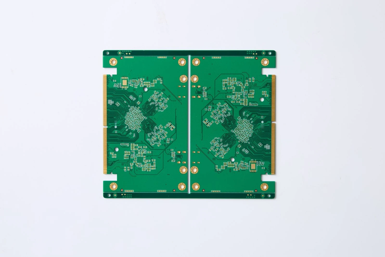
Figure 1. Appearance of a board from a ten-layer multilayer PCB project.
When board area is limited and many connections are needed, inner layers can carry more routing or serve as ground or power planes. Industrial control boards and computing modules may have these needs. The benefit of adding copper layers depends on whether sensitive signals have suitable reference planes nearby and whether return current can flow continuously.
If a double-sided board can already meet routing, electrical, and mechanical requirements, there is a good reason to keep that structure. With more layers, inner-layer patterns are buried, so layer-to-layer registration and via connections need control. Before choosing a multilayer PCB, state what problem the extra copper layers should solve.
The stack of a multilayer printed circuit board combines core and prepreg materials, which serve different roles. A core is fully cured and usually copper-clad on both sides. Prepreg contains resin that has not fully cured, so it bonds layers together. After processing, the copper foil becomes the required circuit patterns or planes.
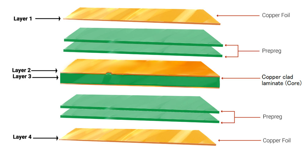
Figure 2. Diagram of the copper foil, prepreg, and copper-clad core stack.
The inner-layer circuitry is formed on the cores before lamination. The cores, prepreg, and outer copper foil are stacked in order. Heat makes the resin flow into gaps between copper features and then cure. The finished dielectric thickness depends on the prepreg type and adjacent copper surfaces; it cannot be worked out by counting prepreg sheets alone.
In a four-layer board, “four layers” means four conductive copper layers; prepreg is not counted. A core usually has copper on both sides, so one core is not the same as one copper layer. When reading a stackup, follow it from L1 downward and note which entries are copper and what material sits between each copper layer.
S usually denotes a signal layer. G denotes a ground plane, and P a power plane. Labels such as L1 and L2 show the order from top to bottom; the design still determines which net each layer serves.
Four-layer boards often use both outer layers for signal routing. The two inner layers may be split between ground and power or both used as ground references, changing how the outer signals are referenced. When comparing a 4-layer PCB stackup, check which layer sits next to each critical signal. If a power plane is adjacent, check whether it is continuous and how it connects to ground at high frequency.
When a design grows from four to six layers, the two added layers can carry routing or serve as reference or power planes. The S/G/P/S/G/S order in Figure 3 is one option. For a 6-layer PCB stackup, inspect the reference plane next to each signal layer. A signal that changes layers also needs a continuous return path.
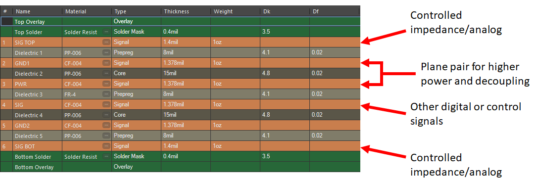
Figure 3. One six-layer functional assignment: S/G/P/S/G/S.
Before choosing an 8-layer PCB stackup, list the problems that the four- or six-layer design has not solved. Is there too little room for routing, or is a suitable reference or power plane missing? Check whether the added copper layers address those needs before accepting the added fabrication requirements.
FR-4 is a class of glass-reinforced epoxy material. Different FR-4 grades can have different dielectric properties and loss. For PCB material selection, check whether the specific grade meets the project’s signal and operating conditions; the FR-4 label alone is not enough.
Finished board thickness is the thickness of the bare board after fabrication. The distance from a signal layer to its reference plane is a different dimension. Two stackups can have the same total thickness but different core, prepreg, and copper-thickness combinations. Keep total board thickness separate from layer spacing when discussing impedance.
One ten-layer board record lists FR-4 KB-6165. It gives 1.2 mm as the nominal finished thickness; the process traveler lists 1.1 ± 0.075 mm as the lamination-stage thickness. These values apply to different stages: the finished board and the lamination operation. Table 1 lists four 0.17 mm cores including copper, plus the quantity and stated thickness of PP1080 and PP2116. Resin flows during lamination and affects the final dielectric dimensions, so review the material record separately from finished-board requirements.
Start by identifying the reference layer for each signal layer. An outer-layer microstrip usually references a nearby inner plane, while an inner-layer stripline sits between two reference planes. When submitting PCB impedance control requirements, specify the target impedance along with trace width, copper thickness, and reference distance so the calculation can account for the finished trace cross-section and dielectric conditions.
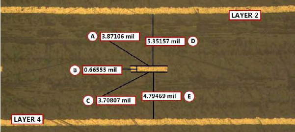
Figure 4. Trace cross-section and measurement locations for adjacent reference copper layers.
Signal current travels forward, while return current needs a closed path. At high frequencies, return current tends to follow a low-impedance region near the signal trace. Maintaining a continuous reference path for high-frequency return current helps limit loop area. If a plane has a long slot or gap, return current may detour and increase electromagnetic-radiation risk.
When a signal changes layers through a via, its reference plane may change too. Check the high-frequency connection between the original and new reference planes. A power plane can carry AC return current, but its connection to the reference network and decoupling also matter. Mark these relationships clearly so layout and fabrication can be discussed against the same stackup.
In the multilayer PCB manufacturing process, inner-layer circuitry is made on the cores first. The copper surfaces are cleaned and imaged. After development, etching removes excess copper to leave the required circuits. The copper-layer data must belong to the same approved revision as the drill, solder-mask, and outline files.
After the inner-layer circuitry is inspected, the cores, prepreg, and outer copper foil are stacked in order, then bonded under heat and pressure. For a conventional mechanical through-hole structure, holes are drilled through the laminated board. The hole walls are prepared and metallized so designated copper layers can connect. Figure 5 shows equipment used in this processing stage.
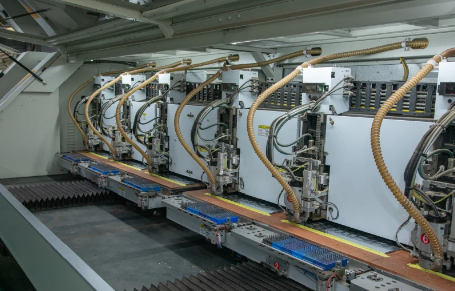
Figure 5. Drilling equipment and the board-processing area.
After the outer-layer circuitry is complete, the board receives solder mask, legend, and surface finish as required by the project. The outline is then machined and the bare board inspected. With blind or buried vias, some layer groups may need processing before a later lamination cycle. The layers a via connects must therefore be defined together with the manufacturing sequence.
Inspection happens at different stages. Inner-layer automated optical inspection (AOI) compares copper patterns; bare-board electrical testing checks network continuity and isolation; final inspection checks the outline and board-surface condition against the mechanical drawing and finished-board requirements. Each check covers a different item and should use the approved files that apply to it.
When comparing two quotes, check whether both use the same board thickness, material, and hole structure. More copper layers add inner-layer patterns and material and require control of registration across more layers. Price cannot be estimated from layer count alone. Even two eight-layer boards may require different fabrication arrangements if their structures or finished-board requirements differ.
If standard through-holes provide the required connections, blind, buried, or microvias may not be needed. These structures can involve staged lamination, additional drilling, or via filling. Start with connection density and routing needs, then decide whether the added processes are necessary.
Materials and finished-board requirements also change fabrication conditions. With a low-loss material, check the specific grade. For thicker copper, review how it affects fine-line processing. Tight board-thickness tolerances or a special surface finish should be stated before ordering. If these requirements change, update the manufacturing data and inspection criteria too.
Before sending an engineering package, review the layer files, drill files, and stackup together. Do the layer names in the Gerber or ODB++ data match the stackup? Do the drill files identify hole types, sizes, and start and end layers? Does the board outline match the current mechanical drawing? Check revision numbers so files from different versions are not included in the same archive.
For controlled impedance, identify each target value, signal layer, reference plane, and tolerance. State trace width, spacing, and any permitted adjustment in the relevant files. Mark the locations and fabrication extents for blind or buried vias, resin-filled vias, or panelization, then check them in a pre-fabrication DFM review. Changes that affect electrical behavior or mechanical fit still require design approval.
When requesting multilayer bare PCBs from GemTech PCB, provide the layer count, material preferences, board thickness, copper thickness, main hole structures, quantity, and outline requirements. These details provide a starting point for a bare-board fabrication quote. If the project has impedance or special-via requirements, confirm the complete stackup before production. Mark any files that are still pending.
Not always. The combination of core, prepreg, and copper thickness affects the finished thickness, so copper-layer count alone does not determine it. Compare the finished-thickness requirement for each option.
No. Standard through-holes can connect multiple copper layers. Consider blind or microvias only when the connection density or routing needs call for them, and confirm the required fabrication steps.
Yes. The specific FR-4 grade must meet the project’s electrical, temperature, and fabrication requirements. Once confirmed, record the grade and material combination in the stackup.
An initial quote can start with the layer count, material preferences, finished thickness, and any special requirements. If impedance or special via structures are involved, confirm the complete stackup and reference relationships before production.


