
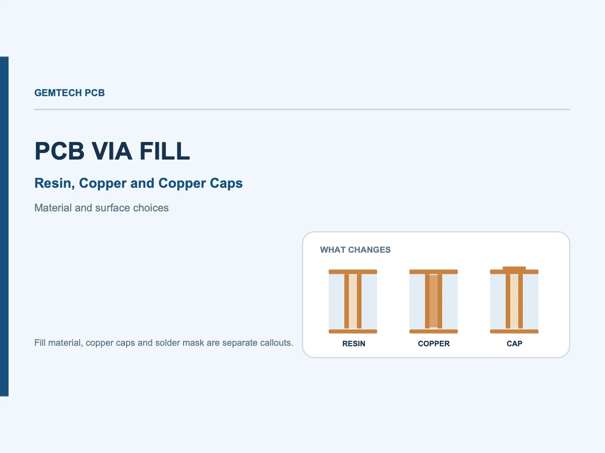
PCB via fill means placing a specified material inside the via cavity. The term alone does not say whether the fill is conductive, whether the barrel already has copper, or whether a copper cap is added at the opening. Resin fill, copper fill, and copper capping affect different locations. When reviewing the process, separate the conductive path in the barrel, the material inside the hole, and the treatment at the opening. Then state the requirements by via type, location, and downstream connection.
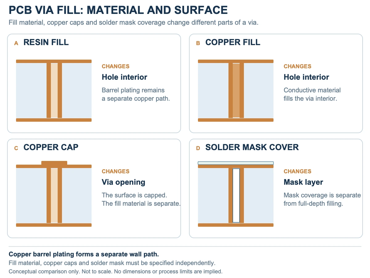
Figure 1. Conceptual cross-sections of non-conductive resin fill, copper fill, fill with copper capping, and solder mask coverage. The diagrams show material locations only and are not to scale.
Barrel copper, material inside the via, and the surface layer at the opening are three different locations. Barrel copper forms the conductive path between layers along the hole wall. Fill occupies space inside the hole. A copper cap covers the opening. Solder mask coverage applies solder mask over the surface opening. If a drawing says only via fill, the fabricator cannot tell which material, barrel condition, or surface layer is required.
Altium's description of HDI via metallization links barrel metallization to layer-to-layer electrical interconnection. Filling the cavity with non-conductive resin does not replace the existing barrel copper. If the design requires a conductive via wall, the fabrication data must still specify the barrel copper. Whether the fill also conducts must be stated separately.
Material inside the hole does not show that the opening has been closed. Resin may stop near the opening or be planarized later. A copper cap is a separate copper layer at the opening, and solder mask is another material layer. The three treatments differ in location, material, and function. Do not use via plug as a substitute for specifying all three.
With non-conductive resin fill, resin occupies the cavity while the existing barrel copper continues to carry the layer-to-layer current. Resin fill and barrel plating have different functions. Resin in the cavity does not remove the electrical requirement for barrel copper, and the resin itself is not a conductive core.
Resin fill occupies the cavity and can provide a base for later surface treatment. If a pad surface is needed above the via, the manufacturing route must account for the order of filling, curing, copper capping, and planarization. Altium's description of the VIPPO process includes non-conductive fill, curing, copper capping, and planarization. Requirements still need to be confirmed for each via type and route.
Do not identify the material only as resin. State whether the fill is conductive, which holes receive it, and whether the opening must remain open, be planarized, or be covered. Copper-filled conductive resin and non-conductive resin are different material conditions and need separate acceptance criteria.
Copper fill places conductive material in part or most of the via cavity. It differs from via-wall plating, which forms a copper layer on the hole wall. Altium's microvia information lists copper plating and copper-filled resin as fill methods. These are general technical categories. State which method the project uses instead of writing only copper via fill.
Copper fill is not the same as plating the via wall. Wall copper forms the conductive path along the hole. Copper fill brings conductive material into the cavity. A drawing that specifies only via-wall plating does not say whether the cavity is filled. A drawing that specifies only copper fill does not say whether the via wall or target-layer connection meets the design requirement.
A board can assign different treatments to different via groups. For example, a through via outside a solder pad may be specified as open or covered by solder mask. A via in a solderable pad may be listed separately with its fill and capped side. A stacked microvia group should be checked by target layer pair, including whether the lower via needs fill and where the next via lands. This example shows that fill can be assigned selectively to different via groups. It does not mean the whole board uses one process. The staggered and stacked microvia structures have a separate explanation of their inner-layer connections.
Fill and capping sides must be specified separately. For single- or double-sided copper capping after fill, state which side receives the cap. Copper capping without fill is a different combination of cavity and opening treatments. The word capped does not say how the other side is treated. The word filled does not mean both sides are capped. Unfilled and capped is not the same structure as filled and capped. State each side's requirement in the fabrication notes or a local drawing.
Copper-containing fill or copper plating changes the material inside the via, but it does not by itself prove the board's current-carrying capacity, thermal performance, or reliability. Current flow also depends on the barrel, fill continuity, connected copper area, and actual net. Thermal performance also depends on the structure and operating conditions. This article explains material location and connection mechanisms; it gives no unverified performance values.
In English sources, via filling can refer generally to material placed in a via. Copper via filling needs context to show whether copper is electrodeposited or enters the cavity as copper-filled material. When terms overlap, state the material and formation method in the process notes so quoting and acceptance do not depend on guessing from a name.
Copper capping adds a copper layer at the via opening. Fill occupies the cavity. The two requirements may be combined or specified separately. A via can be filled with non-conductive resin and then capped with copper. A continuous copper surface does not prove that the cavity contains copper fill.
Solder mask coverage places solder mask over or across the via opening. Its material and layer differ from a copper cap. Solder mask may hide the opening from the board surface, but it does not show that the cavity is filled or that a continuous copper cap is present. Specify opening coverage, fill, and solderable surface requirements separately.
When a via is placed within a component pad, cavity fill and pad-surface requirements may both apply. Review via-in-pad placement and VIPPO selection separately, then combine the specific material and surface requirements. See the via-in-pad and VIPPO topic. This article does not cover fanout outside the pad; it focuses on where the fill, copper cap, and solder mask are located.
Surface inspection and via-cavity inspection answer different questions. At the surface, an inspector can observe depressions, raised areas, exposed fill, discontinuous copper caps, or solder mask coverage. A board photograph alone cannot show whether the cavity has voids or whether fill reaches the specified location. For each feature, define whether it is an acceptance item, then state the inspection method and sample location.
Acceptance criteria also depend on the structure. For a via in a solder pad, check whether the copper cap is continuous and the pad surface is planar. For a stacked microvia group, check whether the lower fill provides the intended copper target for the upper via. Both structures may use fill, but their acceptance items differ.
A cross-section shows only the local structure at the sampled via. If a board contains both resin-filled through vias and copper-filled stacked microvias, the via IDs, layer pairs, and material labels must match the corresponding via groups. Without a sample plan and acceptance basis for each group, one cross-section cannot serve as evidence for another group.
Assess barrel copper continuity separately from the fill inside the via. Seeing fill in a cross-section does not by itself prove that the conductive barrel path is complete. A copper cap at the surface does not prove that the cavity contains copper fill. If electrical connection, cavity fill, and surface condition are all delivery requirements, define the document and acceptance basis for each one.
Specify the barrel's conductive path, the material inside the via, and the treatment at the opening separately. Bind each requirement to a defined via group. The fabricator should be able to identify the via type, fill, copper cap, and solder mask coverage for each group from the data.
Before sending the data, group vias by hole number, net, or defined area. Then list the via type and treatment for each group in the via table or fabrication notes. Do not combine ordinary vias and selectively filled vias into one undifferentiated requirement.
For each group, state the via type, start layer, and end layer. If the structure has several microvia segments, identify the target layer and connection for each segment. State whether the cavity remains open, is filled, or receives a separate surface treatment.
Name the fill material and state whether it is conductive. Non-conductive resin, electrodeposited copper, and copper-filled conductive material are different requirements. Also state which side receives copper capping, whether planarization is needed, whether solder mask covers the opening or leaves it exposed, and which final surface finish applies.
Define inspection scope separately. Surface inspection may cover depressions, raised areas, exposed fill, or copper-cap condition. For an internal cavity condition, name the via group and inspection basis. Use the same units, coordinate origin, and revision in the via table, drill files, stackup drawing, and fabrication notes.
For multilayer materials and via pairs, see the HDI PCB structure guide. For stacked microvias, confirm how the upper via connects to the lower fill. For pad location and surface requirements, see the via-in-pad and VIPPO topic. For a specific bare-board review, submit the stackup, drill, and fill table through the GemTech PCB HDI bare-board product page.
A board with several via groups can specify them separately. For example, a through via outside a solder pad may be identified as open or covered by solder mask. A via in a component pad can be listed separately with its fill and capped side. For a stacked microvia group, check the target layer pair, whether the lower via needs fill, and where the upper via lands. This example shows selective labeling. It does not mean the whole board uses one process.
An example note could read: “Via group D: specify the fill for this group; copper capping on side A only; state on the drawing whether side B remains open or is covered by solder mask; list planarization and final surface finish separately.” A and B are illustrative side labels. The actual file should identify the corresponding board sides. One-sided copper capping does not mean the cavity is filled, and fill does not mean both sides are capped.
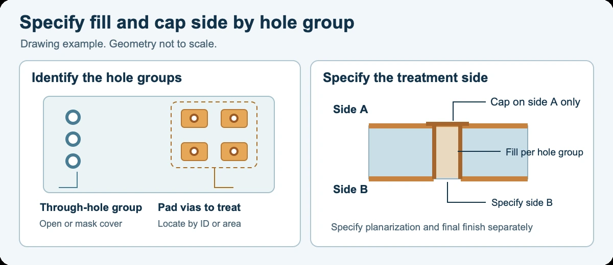
Figure 2. Example markings for local via groups and copper capping on one side. Record the via group, fill, capped side, and the condition of the other side separately. Not to scale.


