
Via-in-pad places a via within the copper area of a component pad. It can be evaluated when routing space around the pad is limited, when a connection needs to change layers at the pad, or when a specified pad is used for an electrical or thermal connection in a particular design. The choice also depends on the pad, via type, nearby routing, and surface requirements. If the via opening lies within a solderable pad, check whether it can contact solder and whether the surface must remain continuous and flat. Under some structures and conditions, an open hole may allow solder to enter the cavity. VIPPO commonly includes filling, copper capping, and planarization. The via structure and project requirements determine which steps are needed; the term via-in-pad describes location and does not set the process.
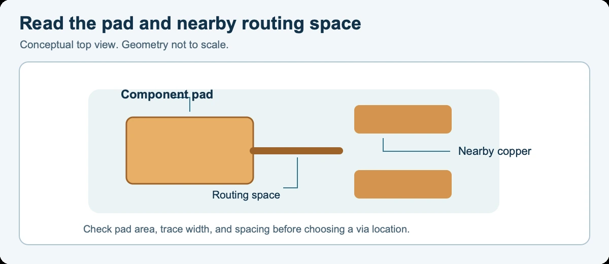
Figure 1. A conceptual top view of a component pad, nearby copper, and routing space. The geometry is illustrative.
A via located within the copper area of a component pad is via-in-pad. Terms such as “PCB via-in-pad” describe location, not whether the hole is through, blind, or a microvia, nor whether the cavity is open, resin-filled, copper-filled, or capped. Design files should specify via location separately from subsequent treatment.
A via may be placed at the center, edge, or near a component pad. Center placement can remove the short trace from the pad, but the via opening then occupies part of the soldering surface. An offset via may still lie within the pad and remain a via-in-pad structure. Evaluate the pad shape, annular ring, and nearby copper clearance against the component footprint.
Via-in-pad can use different via types. Through vias, mechanical blind vias, and laser-drilled microvias may all be placed in a pad, but their layer spans, depths, and opening directions differ. The [HDI PCB structure and via-type guide] explains how to place via layer pairs in the stackup; confirm the actual layer pair in the project stackup and drill table.
When a short trace can route from a pad to a via outside it, [dogbone fanout] can preserve the pad surface for soldering, but it needs room for the trace, via pad, and nearby copper clearances. If there is not enough routing space, evaluate via-in-pad or another specified via layer pair and check the pad-surface treatment. The choice depends on the actual pad, via type, stackup, and surrounding routing. There is no universal ball-pitch threshold for every board.
Via-in-pad places the via inside the copper area of a component pad. It removes the short trace to an outside via, but the via opening also occupies the soldering surface. Check the usable pad area, annular ring and nearby copper clearance, solder-mask opening position, target copper layer, and any filling, copper capping, or planarization requirement.
The via may sit at the center, edge, or another position within the pad. If it remains inside the pad copper, it is still via-in-pad; if it moves outside the pad and connects by a short trace, it is dogbone fanout. When the via opening lies on a solderable pad, check for possible solder contact and whether the surface needs to be continuous and flat. Evaluate the package footprint, via diameter, annular ring, routing, and stackup together.
Dogbone fanout routes a short trace from the pad to a via placed outside it. This preserves the pad surface but uses space for the trace, via pad, and copper clearance. Do not check only the via center; verify that the trace width, via pad, and adjacent copper can all meet the design rules.
If dogbone fanout meets the actual trace-width, via-pad, and clearance requirements, the via can remain outside the pad. If it does not, compare via-in-pad, blind-via, or microvia options. A through via may pass multiple inner layers, with clearances on layers it does not connect to as required by the design; blind vias and microvias span only their specified layer pairs. Keep the related pad, stackup, drill, and fabrication files on the same revision.
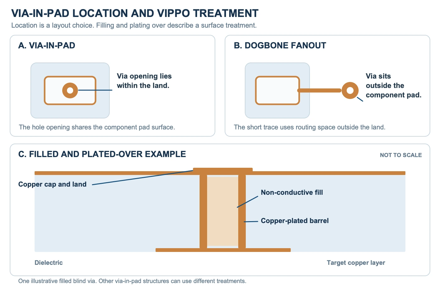
Figure 2. Plan views compare via-in-pad with dogbone fanout. The cross-section illustrates one conceptual via-in-pad structure with fill and a copper cap. The drawing is illustrative and not to scale.
The Altium VIPPO source notes that an [open hole may allow solder to enter the cavity under some structures and conditions] and may change the solder available near the pad or the resulting surface shape. This is a possible effect to evaluate, not an outcome for every via-in-pad design.
The risk depends on via type, whether the cavity opens through the other side, which soldering surface contains the opening, and the assembly conditions. A through-via cavity may extend to the other side, while a surface blind via terminates at an inner layer. Confirm the actual opening-to-pad relationship; do not assume the soldering surface is safe just because the via is labeled through or blind.
If the opening is away from the soldering surface, other manufacturing requirements may control the treatment. If it lies in the pad, flatness and surface continuity have a more direct effect on that pad. Solder-mask coverage, resin fill, and a copper cap use different materials and occupy different locations; one treatment does not automatically replace another. See [the differences between resin fill, copper fill, and copper capping] in the B5 via-fill article.
Do not infer fill requirements from the name blind microvia or stacked microvia alone. Check the microvia termination layer, whether the next segment lands at the same location, whether the opening lies in a solderable pad, and what surface the fabrication drawing requires. For the layer relationships of [staggered and stacked microvia connections], see the B3 article.
VIPPO stands for “via-in-pad plated over” and commonly refers to a via in a pad that is filled and capped with copper at the surface. It names a type of cavity and surface treatment; it is not a synonym for via-in-pad. The design can first specify whether a via belongs in the pad, then define the fill material, cap side, and surface treatment.
[Altium’s description of a typical VIPPO process] includes plating the via wall, cleaning the cavity, filling it with resin or another approved non-conductive material, curing the fill, capping the opening with copper, planarizing the surface, and applying the final surface finish. The exact order varies with via type and fabrication route. The copper cap creates a continuous surface over the opening, while planarization corrects the height difference between the cap and surrounding pad.
Via-in-pad treatment can be applied only to selected pads; do not assume every via on the board needs VIPPO. Design files should identify which pads need treatment, which side is treated, the fill material, and the required surface condition after capping. “Via-in-pad,” “plugged,” or “capped” alone does not define these details.
For microvia or stacked-via connections, the fill also affects the next segment’s landing and interface. Resin fill and copper fill are not interchangeable merely because both occupy the cavity, and a surface copper cap does not identify the internal fill. Record the material, via layer pair, and surface layer separately for manufacturing review.
A manufacturing-ready via-in-pad note should answer three questions: which pad or area contains the via, which layers the via connects, and what treatment is required inside the cavity and at its opening. Record via location, via type, and surface treatment separately so the fabricator can check the connection span and treatment scope.
One board may include open vias, vias covered only by solder mask, and pad vias that need filling and copper capping. Separate these treatment groups by hole number, net, or specified region. This avoids treating every via-in-pad as a whole-board fill requirement or applying VIPPO by default to ordinary holes.
For each group, list the hole or region, via type, diameter convention, start layer, and end layer. If a pad connection uses multiple microvia segments, show the target copper and the connection between segments one segment at a time.
State the fill material and whether it is conductive. Identify whether resin is non-conductive; for copper fill, specify electroplated copper or copper-bearing conductive fill. Mark which surface is capped, whether planarization is required, and the final surface finish. Also identify holes that remain open, receive solder-mask coverage only, or require fill and cap, so groups do not share an unstated default.
For a specific bare-board project, submit the stackup and via table through [GemTech PCB’s HDI bare-board product page] and arrange pre-fabrication review according to the via type. If the project does not require vias inside pads, compare dogbone fanout and other interlayer connection options first.
The drawing fields should include the hole number or region, via type, diameter convention, start and end layers, target copper at the via bottom, fill material and conductivity, cap side, solder-mask coverage or opening, planarization and surface-finish requirements. Keep the hole table, Gerber or ODB++, drill files, stackup drawing, and fabrication notes on the same units, coordinate origin, and revision.


