

To choose a standard PCB thickness, first fit the board to its connector, slot, mounting method, and enclosure. Then specify the finished total thickness, tolerance, and measurement basis. Use a common nominal thickness as a starting point, then compare it with the dimensional limits at the mating interface. If a stackup change alters the material, copper thickness, or spacing between dielectric layers, recheck the affected holes and controlled-impedance requirements.
This article explains thickness selection and fabrication documentation for rigid bare boards. Flexible, rigid-flex, and special constructions require review against their specific stackup and mechanical drawings.
A nominal thickness of 1.57 mm is common for rigid boards, while other thicknesses are used for different constructions. The chosen finished thickness must satisfy the mechanical interface and fit the intended stackup.
When choosing a standard PCB thickness, first check whether a connector, slot, screw mount, or enclosure limits the board. If the interface sets a fit range, treat it as a design input. If the structure leaves room, confirm with the manufacturer a finished thickness that suits the layer count, materials, and copper requirements.
Set the finished thickness to meet the tightest mating interface first. Slots, edge connectors, standoffs, and the enclosure can all constrain the board. For an edge connection, use the thickness at the insertion area. A reading from the board center describes a different location.
Nominal thickness is the target. Actual measurements must use the same measurement basis. The drawing should specify the measurement area, measurement points, the surfaces on both sides, and whether surface finish or solder mask is included. In the 1.57 mm example, surface-finish plating, solder mask, and conformal coating, where applicable, are included in the total. State the actual measurement surfaces and included layers in the project drawing.
For selecting the treatment itself, see our PCB surface finish selection guide.
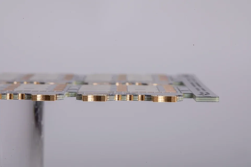
Figure 1. Side view of PCB panel edges showing the visible copper and dielectric edges.
Measure finished board thickness between the surfaces at the points defined in the drawing. Local dielectric spacing is the insulation distance between adjacent copper layers. Controlled-impedance traces depend on the local distance from the trace to its reference plane. The overall board thickness describes a different dimension.
In one four-layer FR-4 example, the prepreg thickness sets the trace height above the ground plane. The stackup total separately accounts for copper, core, and prepreg. These dimensions are related within one stackup, but they require separate calculations.

Figure 2. Schematic of finished board thickness and local dielectric spacing. The diagram is not to scale. The drawing defines the measurement surfaces and points.
When total board thickness changes, check whether the signal layer, reference plane, or dielectric boundary between them moves as well. If local spacing, copper thickness, or dielectric properties change, recalculate the affected impedance structures using the new stackup.
In a multilayer rigid board, core and prepreg serve different roles, and their thickness definitions must be kept clear. A core is a fully cured laminate that may have copper foil on one or both sides. Prepreg is glass cloth coated with partially cured resin. During lamination, the resin bonds the layers together.
During lamination, heat causes prepreg resin to flow into spaces between adjacent copper areas. Pressure can also force some resin out at the board edges. This changes the pressed dielectric thickness. Use the pressed value in the final stackup. The raw prepreg thickness on a material datasheet refers to the material before pressing.
For an initial estimate, list the core thickness (first confirm whether it includes copper), the prepreg dielectric thickness after lamination, and any copper foil not already included in the core value. If the core entry gives the total thickness of a copper-clad core, do not add its copper foil again. Include surface finish and solder mask according to the measurement basis defined on the drawing.
Through-hole aspect ratio compares board thickness with hole diameter. The fabrication data should state whether the calculation uses the drilled diameter or finished hole diameter. A thicker board or smaller hole increases the ratio, so review the hole type, hole-size definition, and plating conditions together.
For controlled-impedance calculations, use the trace geometry, board stackup, and material dielectric parameters together with trace width, copper thickness, and local dielectric thickness. If a thickness or material change alters any of these inputs, recalculate the affected lines against the new stackup and impedance target.
If a change only affects a board area unrelated to controlled-impedance traces, compare the old and new stackups to confirm whether the local geometry is unchanged. Then determine which impedance structures need to be recalculated.
RFQs and engineering review documents should state the mechanical target, finished-thickness measurement basis, material stackup, and allowed adjustments in the same document revision. A target thickness alone does not show whether the mating area, tolerance, and stackup agree.
For layer order and material placement, see our Multilayer PCB Stackup Guide. Before sending files, use the PCB DFM Checklist Before Manufacturing. Once the project requirements are defined, submit the thickness specification, stackup, and mechanical drawing through our multilayer bare-board manufacturing and quotation page.


