
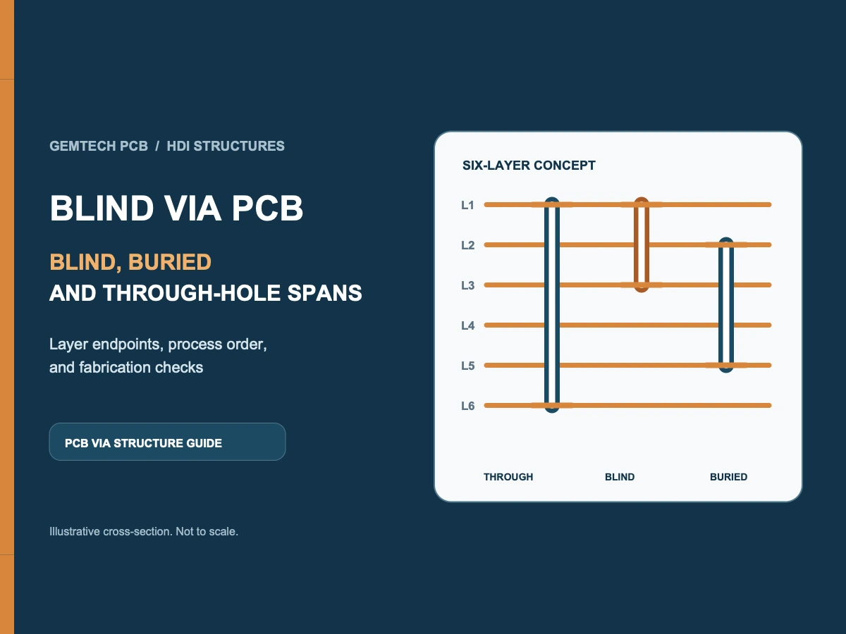
For a blind via PCB structure, specify the start and end layers for each via type and the copper layers that must connect, then check them against the stackup and process stage. A blind via connects a board surface to a specified inner layer and ends there. A buried via connects two inner layers and does not reach either finished outer surface. A through via spans the full board. Blind and buried describe a via's layer span, while microvia describes a short-span structure, so a microvia can also be a blind via.
This article explains how via spans are specified in fabrication data. BGA pad space and total layer count are conditions to compare, but neither determines the via type on its own. The article covers bare-board fabrication review. It does not provide circuit-design services.
A blind via starts at an outer layer of the finished board and ends at a specified inner layer. A buried via connects two inner layers and has no opening on the finished outer surfaces. A through via extends from one surface to the other. The name tells you where a via starts and ends. Whether it connects to copper on every layer it passes through depends on the connection pads and clearance settings.
Show each layer pair on the stackup drawing, such as L1 to L3 or L2 to L5. The end layer changes the via depth and the manufacturing sequence.
Blind and buried vias are classified by their endpoints and whether they reach a board surface. Microvia describes a short-span connection structure. An outer-layer to next-layer microvia can also be a blind via. Distinguish the two terms and check the via type and its start and end layers separately. They are not mutually exclusive options.
Via span and treatment at the pad surface are separate specifications. The layer spans of blind and buried vias identify which copper layers a finished hole connects. Via-in-pad plated over (VIPPO) describes treatment of a via placed in a component pad. The VIPPO filling, copper capping, and planarization steps address the via cavity and component-pad surface. For example, a through via that spans L1 to L6 can sit in a component pad and be filled, copper-capped, and planarized to form a continuous, solderable surface. It still connects both board surfaces. A copper cap does not turn a through via into a buried via. Fabrication files should list the via's start and end layers separately from its via-in-pad treatment.
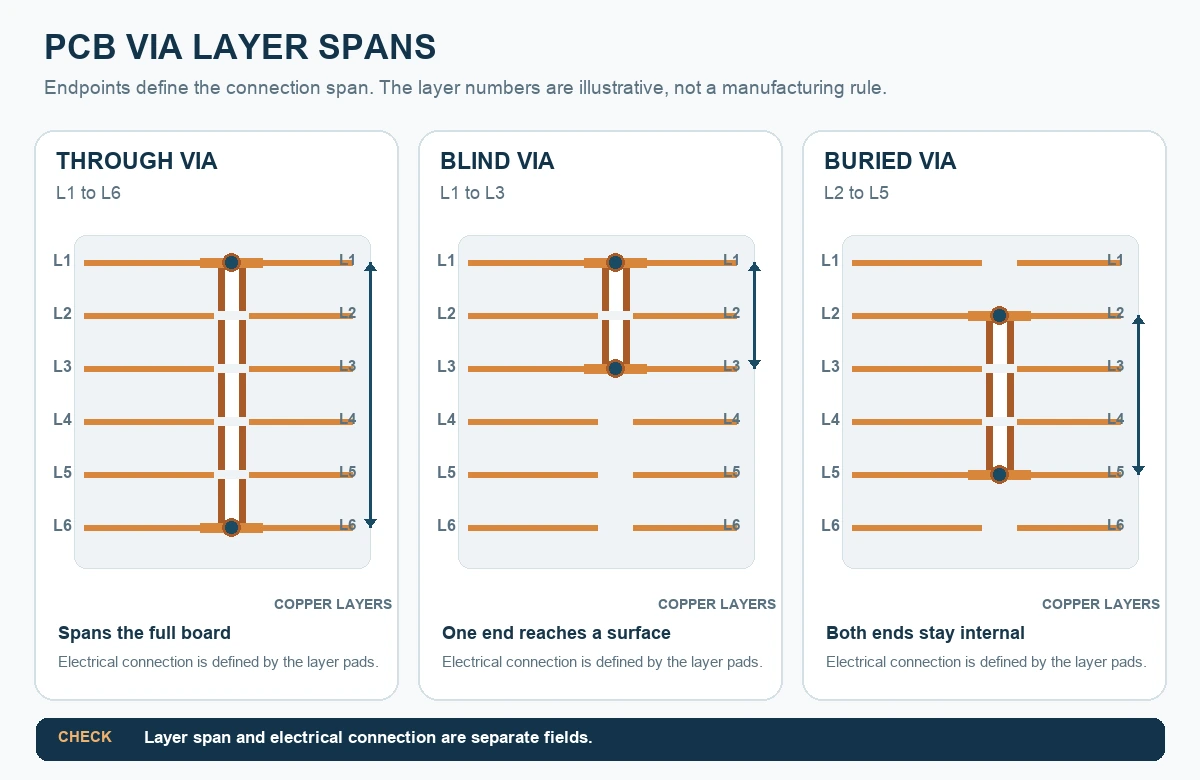
Figure 1. Layer spans of through, blind, and buried vias. Layer numbers are illustrative, the drawing is not to scale, and it does not represent a fixed factory stackup.
The layer count only tells you how many copper layers the board has. It does not show which layers each net must connect to. The same multilayer board may use through vias only or add blind, buried, or microvias for selected connections. Start with the electrical connection task, then check the via structure against the stackup.
In a hypothetical six-layer board, if a signal only needs to connect from L1 to L2, a through via still passes through the other layers. An L1-to-L2 blind microvia would not pass through the later inner layers. This compares two structures for the same connection task. The layer numbers are illustrative and do not describe a measured project or a manufacturing capability.
BGA package pitch and escape routing for inner rows can affect fanout. If a through-via pad and its clearance take up a routing channel, blind vias or microvias can be candidates. If through vias still reach the target layers and leave the required routing space, a through-via option may meet the goal. A package name alone does not establish that an HDI via type is required.
If a net must connect L1 to L3, an L1-to-L2 blind microvia completes only one segment. A second connection is needed from L2. A staggered arrangement needs a routing trace on the intermediate copper layer; a stacked arrangement needs a continuous copper connection surface between the via segments. Replacing the original through via with a smaller opening does not complete the path by itself. BGA fanout and via-type selection must therefore be checked against the target layer and required connection segments. For board-level tradeoffs, see HDI structure selection and pre-fabrication review. For details on the microvia bottom connection across a short layer span, see the separate topic.
Mechanical or laser drilling describes how a via is formed. Blind and buried describe its start and end layers. These are separate classification axes. Short-span microvias are often laser-drilled, but diameter alone does not make every small hole a microvia. The term blind via alone also does not identify the drilling method.
A mechanically drilled blind via can span an inner-layer section. An outer buildup microvia needs a dielectric and bottom-copper target suited to that structure. Material choice and lamination sequence can affect via formation. The manufacturer should assess actual hole-size boundaries, permitted dielectrics, and tool conditions against the specific stackup, rather than applying one web-page threshold.
For each drill group, state the via type, start layer, end layer, and diameter definition. If multiple layer pairs share a drill file, separate them in a layer-pair table or attribute list so one drill symbol does not refer to different connections.
A microvia also needs a target copper layer at its bottom and a landing pad. If an upper via must land on a specified copper layer, check pad size, registration tolerance, and via structure against the same file revision. These are fabrication-data requirements. They do not include choosing circuit connections or providing board-level design services.
Via length, diameter, and aspect-ratio definitions for a blind via change with the layer span. Before comparing mechanical holes and microvias, confirm whether via depth means the full board thickness or the local dielectric span. Then confirm whether the denominator uses tool size or finished hole diameter. For more detail, see the article on via aspect ratio.
The process sequence depends on when each via can be formed and whether later lamination will close access to it. If an inner-layer via becomes inaccessible after more layers are added, form and metallize it before it is covered. An outer buildup blind via may be formed after additional dielectric is added, followed by the applicable plating and patterning steps. Different stackups may use different routes.
A useful review starts by identifying the core and buildup layers, then locating each via's target copper layer within the sequence. For an inner-layer via that will soon be covered, review whether it needs filling or surface treatment for later lamination. A via formed on the outermost layer and not covered by another lamination step may need different treatment. Confirm each item against the specific structure and process.
The sequential buildup and via metallization process can include staged lamination, via formation, and plating. Inner-layer and outer-layer vias may receive different treatment. The fabricator should check when each via is formed relative to later material coverage and whether filling or surface treatment is required. Different stackups can use different routes.
After the layer order is set, the fabricator must confirm that the drill layer pairs and lamination revision agree. Covering a via too early can make the target layer hard to reach. Omitting later coverage or surface-treatment instructions can also leave the finished structure different from the intended one. See the HDI sequential lamination and via formation route for a separate explanation of staged lamination.
A through via passes through intermediate layers and uses routing space. Blind or buried vias shorten part of a connection span, but can add separate drilling, lamination, registration, plating, or filling steps. Calculate cost for the complete structure and its requirements. Do not apply a fixed surcharge based on the via name.
When comparing options, hold the connection task, target layer, and board-thickness conditions constant. Then compare which layers each via occupies and which process steps it needs. If a shorter via span adds lamination steps or dedicated drill groups, calculate the net cost from the actual route. This article does not state an unverified price multiple or manufacturing limit.
Hole diameter is not a stand-alone manufacturing cost measure. Effective depth, tool size, target pad, copper requirements, and layer spacing all affect review. If a drawing does not state the diameter definition, a quote may not correspond to the same via structure. See the via depth and diameter definitions for aspect ratio.
Before releasing fabrication data, put the stackup drawing, via layer pairs, drill table, and process notes on the same revision. The labels blind via or buried via alone do not tell the fabricator where a via starts, where it ends, or how later lamination will treat it. Use this sequence for the review:
After confirming the files, review the published product scope on the HDI bare-board manufacturing and review page, then submit the stackup and drill data through the HDI project quote form. Include the revision, quantity, and open questions for review. Drawing changes and quotation discussions do not replace the design team's formal structure approval.


