
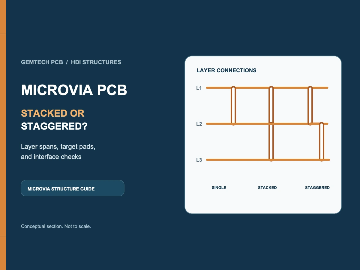
A PCB microvia connects a start copper layer to a target copper layer across one short dielectric span. To compare microvias, first identify the target copper at the bottom of the hole. If the signal continues to another layer, check how the next via segment connects. Segments may align vertically to form a stack, or shift laterally and connect through a pad or short trace on an intermediate layer. Check the hole diameter, dielectric span, and interface together in the same stackup.
In this article, “single segment” is a teaching description of a connection relationship, not a replacement for a standard term. If a project cites a standard or customer definition, confirm the exact via layer pair and measurement convention against that revision.
A microvia is a short connection across a defined layer span. It passes through the specified dielectric from near its start copper layer and terminates at the target copper layer. Evaluate the via segment together with its target pad and connected trace. A single hole-diameter value is not enough.
The fabrication package should identify the applicable standard or customer definition and its revision. If the project does not provide a definition that can be applied directly, show the via start layer, end layer, and dielectric span in the stackup drawing or fabrication notes so the fabricator can review them against the actual process.
Microvias are commonly formed with laser drilling, but the label “laser-drilled hole” does not fully describe the structure. Material, hole depth, target copper, and later processing all affect how a via segment is formed. Mechanical holes, blind vias, and microvias are distinct concepts. A small-diameter mechanical hole is not automatically a microvia.
A microvia may also be a blind or buried via. These labels describe different aspects of the connection. Blind and buried vias describe a span from a surface to an inner layer, or from one inner layer to another. A microvia describes a short interlayer connection. The [layer spans of blind and buried vias] help identify the opening and termination layers. The [HDI structure selection and pre-fabrication review] considers these vias within the full board stackup.
BGA pad pitch and available fanout routing can affect microvia options, but they are only evaluation conditions. Total layer count, component type, or the “HDI” label alone cannot determine whether a design should use stacked or staggered vias. This article focuses on fabrication documentation and design-for-manufacturability checks, not circuit-design services.
A single-segment microvia connects a start layer to a target layer. To continue to a deeper layer, another via segment can align with the first in plan view to form a stack, or shift laterally and connect through a pad or short trace on the intermediate copper layer. Compare the target surface of each segment and how adjacent segments connect.
In stacked microvias, the bottom of the upper segment lands on the connection area of the lower segment. The upper and lower segments are not one continuous long hole. They are separate segments joined through an intermediate copper surface. The fabrication package should identify the lower segment’s termination copper, the upper segment’s start location, and the connecting copper surface. “Two stacked levels” or one total depth does not provide those details.
In staggered microvias, the centers of the upper and lower segments are offset. The signal passes between them through a pad or short trace on the intermediate layer. Staggering moves the vertical interface, but it requires enough connection space on that layer. The same layer number does not mean the vias share the same lateral position. The design files should show the via locations and intermediate path.
Review [interlayer connections for microvias and stacked vias] together with the interfaces between upper and lower segments. Compare routing space, segment count, target pads, later lamination, and manufacturing steps that need confirmation. Whether a stacked or staggered structure is suitable depends on each segment and its target pad. One aspect-ratio or reliability figure cannot decide it alone.
Also trace the signal from its target pad to the next via segment. A staggered design needs a pad or short trace on the intermediate layer. A stacked design needs the lower connecting copper to accept the upper via. Do not decide only because “staggered takes more space” or “stacked is more compact.” Check the actual layer order and interface conditions.
A comparison figure should show both the cross-section and the via locations in plan view. The cross-section shows via depth and target copper. The plan view shows whether stacked segments share a center and where the intermediate route sits in a staggered structure. One view alone leaves the other geometric relationship unclear.
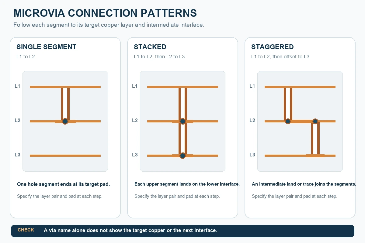
Figure 1. Conceptual cross-sections of single-segment, stacked, and staggered microvias. Layer numbers and positions are illustrative. The drawing is not to scale and does not represent manufacturing limits.
The bottom of a microvia must land on the designated target copper surface to make the intended interlayer connection. The files should identify the start and end layer of each segment and the pad or connection area on the target copper. Metallization on the via wall forms the conductive path. The bottom landing determines which trace or copper layer the segment connects to.
For a single-segment microvia, check whether the bottom landing matches the target pad, whether the connected copper layer joins the trace, and whether clearance around the via meets the design rules. If the target layer or net is unclear, the fabricator cannot infer the intended connection from the board layer count alone.
In a stacked structure, the target surface of the upper microvia is usually the connecting copper surface of the lower segment. In a staggered structure, the two segments need an intermediate pad or trace. Because the interfaces differ, list each segment separately in the drill table. Do not combine all holes into one diameter group without layer-pair information.
If a microvia sits inside a component pad, its location also involves via-in-pad processing. Specify [via-in-pad and pad placement] separately. Filling, copper capping, and planarization are pad-surface requirements; they are not automatically included by the word “microvia.”

Figure 2. Interface of a single-segment microvia landing on target copper, with h/d symbols showing the relationship between segment depth and via diameter. The symbols are illustrative, and the drawing is not to scale.
The target copper surface also defines the connection task. If the via bottom connects to a plane or power plane, the files should state the electrical connection and net. Do not infer the connection from via location alone. A dot marking the via bottom in a diagram cannot replace the actual mapping in the drill table and stackup drawing.
Whether a via needs filling depends on its location, the later structure, and the final surface requirement, not on the word “microvia” or “stacked.” Fabrication notes should identify which holes need filling, the fill material, whether copper capping is required, and whether the surface must be prepared for a later connection or soldering.
If a via is placed directly inside a component pad, the design may specify via-in-pad plated over (VIPPO), which fills the via and then caps it with copper. Specify [VIPPO filling, copper capping, and planarization] according to the pad surface and later assembly requirements. This treatment should not be extended to all microvias.
Via formation and metallization in sequential buildup must follow the lamination sequence. If an inner-layer via will be covered by a later lamination cycle, the process may require the relevant treatment first. Some outer-layer vias may follow another route and remain open. The actual sequence depends on segment location, later lamination, and the target surface for an upper via. See [via formation and metallization in sequential buildup] for more on this process. For the overall order, see [the sequence of lamination and microvia formation].
Specify filling, copper capping, and planarization by via group and surface use. Do not treat “blind microvia” or “stacked microvia” as a uniform fill instruction. Fabrication notes should identify the holes to be filled, the material, copper-cap coverage, and target surface. See [via filling and copper capping] for more on these options.
Assess a [microvia aspect ratio] by comparing the dielectric span of one via segment with its corresponding via diameter. Do not divide total board thickness by the diameter of a single microvia. For a structural illustration, h/d represents the ratio between that segment’s dielectric span and its via diameter. Here, h is the dielectric span of the segment, and d is the via-diameter convention specified in the engineering files.
If two via segments are stacked, record h1/d1 and h2/d2 separately. Comparing each segment shows how much dielectric it spans. Adding the two depths and dividing by one diameter can hide a longer upper or lower segment. This symbolic relationship explains how to read the drawing; it is not a standard limit or a manufacturing guarantee.
The via-diameter measurement convention also needs to be stated. Design files may specify a tool diameter, an opening diameter, or a finished hole diameter. These refer to different stages before and after fabrication. Before quoting, confirm the field, unit, and measurement stage for h and d, and keep the via layer pairs, dielectric spans, and drill data on the same revision.
Any project limit for microvia aspect ratio must be confirmed for the via type, material, depth, and acceptance conditions. Do not derive it from another board or from a mechanical-hole criterion. For more on calculation conventions, see [single-segment depth and via-diameter conventions for aspect ratio], then check the standard revision approved for the project.
The fabrication package should make the start, end, target copper, and later processing clear for every via segment. Show these relationships in the stackup drawing, via layer-pair table, and fabrication notes, then check the following items:
After the structure is finalized, review the product scope on the [HDI bare-board manufacturing and review] page. Submit the same-revision stackup drawing and via layer-pair table through the [HDI project inquiry] link. Include the via-segment drawing, target copper, and surface requirements so the fabricator can assess the specific structure instead of quoting by layer count or microvia count.


