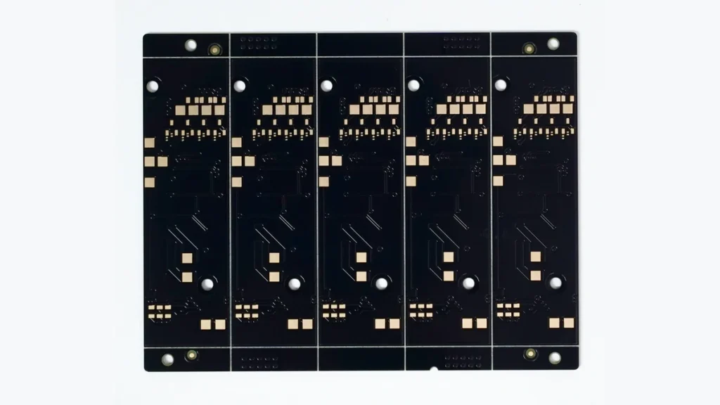
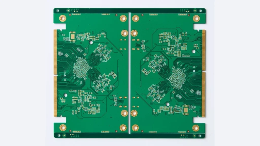
Start with signal and reference-plane relationships. Then compare two 8-layer assignments and read the core, prepreg, dielectric-gap, impedance, and drill records.
Compare signal, ground, and power layer options, check reference paths and dielectric spacing, and review project-specific material and lamination data before requesting a quote.
Compare two four-layer sequences by the reference beside each outer signal, the room left for power, and the return path at a layer change. Then separate total board thickness from signal-to-plane spacing and prepare one matching fabrication package.