
GEMTECH PCB
For a 6-layer PCB stackup, start with the main constraint in the existing four-layer layout: insufficient signal-routing space, reference planes that do not suit critical nets, or too little copper area for power. Assign the two added copper layers to those needs, then check reference paths, dielectric spacing, and materials. The role of each layer depends on the selected stackup, so total board thickness or layer count alone does not determine suitability.
Before adding two layers, identify what the four-layer board cannot accommodate. If signal routing is the main constraint, add a signal layer. If critical nets need a more suitable copper reference, evaluate an added ground reference layer. If the copper area for power is insufficient, reserve a power layer or a copper region for power.
Record the layer and reference plane for each critical net, and note how the power nets are distributed. If the four-layer layout still has conflicts, compare its reference-plane and power arrangements with the four-layer PCB stackup options, then state which problem the two added layers should solve.
Additional copper layers can provide more space for signal routing, reference planes, or power distribution. Set priorities based on signal edge rates on critical nets, power needs, and component density, then compare 6-layer PCB stackup options.
The three example six-layer stackups below assign three, four, or two copper layers to signal routing. Filter them by the number of signal layers needed, reference-plane locations, and copper area for power. Then check the reference path for each critical signal. The board’s nets and routing needs determine whether a layer order is suitable. For an eight-layer comparison, read the 8-layer PCB stackup guide.
Read the layer order from L1 through L6, top to bottom. S means signal, G means ground reference, and P means power. The selected stackup determines layer assignments and the number of available signal layers. Check component placement, via connections, and routing space to confirm that the layout fits.
The four-signal-layer option keeps both L3 and L4 for signals. Check the spacing between them, nearby traces, and return connections to assess interlayer coupling against the board’s signal requirements. For the two-power-layer option, first confirm the power assignments on L3 and L4. Then check whether the reference planes for the outer signal layers are continuous.
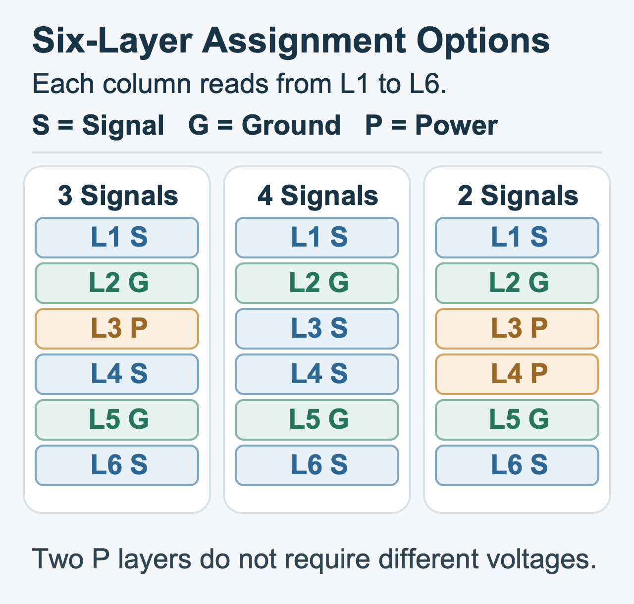
Figure 1. Six-layer stackup examples showing the signal, ground-reference, and power assignments for three layer orders from L1 through L6.
When dielectric spacing changes, review the cross-section again. Check the distance from each signal trace to its reference plane, trace width and spacing, and continuity of the reference copper. Mark the relationship between each signal layer and its adjacent reference plane on the six-layer stackup drawing.
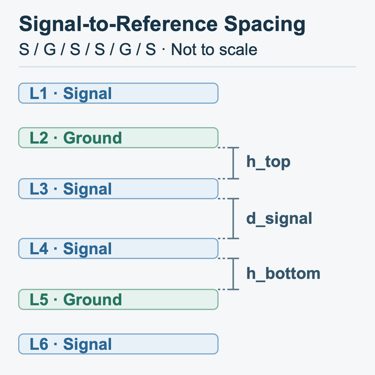
Figure 2. In the diagram, h_top and h_bottom are the reference spacings from L3 to L2 and L4 to L5, respectively. d_signal is the spacing between L3 and L4. Record layer function and each spacing separately. The drawing is not to scale.
Dielectric separates adjacent copper layers. An outer-layer trace and the nearby reference plane form a microstrip structure. An inner-layer trace between reference planes is usually evaluated as a stripline. Because dielectric thickness changes the geometry between a signal trace and reference copper, results from a previous controlled-impedance analysis cannot be carried over without review.
After setting the layer order, check the signal’s return path to its source. TI explains that, as frequency rises, return current follows a lower-impedance path close to the signal trace. A gap in the reference plane can force that path to detour and increase loop area.
When a signal changes layers, check that a low-impedance connection can link the reference layers before and after the transition. If both reference layers are ground, consider placing ground stitching vias near the signal via. If the signal changes from a ground reference to a power reference, also review the power network and decoupling path.
Record the finished-board thickness requirement separately from the thickness requirements at each lamination stage. Then list the core and prepreg labels. One anonymized six-layer HDI project record specifies FR-4 KB-6165, a finished board thickness requirement of 0.60±0.10 mm, one core listed as 0.17 mm including copper, and four PP1080 prepreg plies labeled 0.075 mm each.
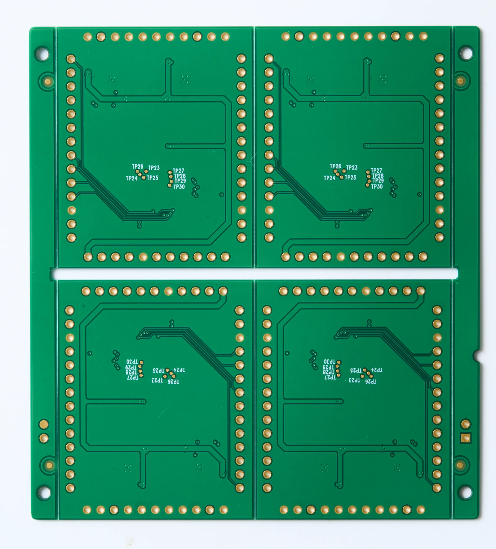
Figure 3. Photograph of a green PCB panel.
The core, prepreg, and copper foil make up the stackup, and lamination bonds them into a board. Count board layers as copper layers. Prepreg (PP) is an insulating dielectric and does not count as a copper layer. Copper cladding on the core and foil added during lamination form the corresponding copper layers. Do not add the PP1080 label thicknesses to derive post-lamination dielectric thickness or finished board thickness.
Complete the DFM review before fabrication, covering copper-layer files, via structure, material dimensions, impedance requirements, and revision control. For the full layer order and material relationships, see the multi-layer PCB stackup guide. When preparing a package for bare-board PCB manufacturing, match the finished board thickness and tolerance, material combination, via connection range, and impedance requirements to the same revision of the engineering files. Include the quantity and any routing conditions that need confirmation when requesting a bare-board manufacturing quote.


