
GEMTECH PCB · STACKUP GUIDE
A 4-layer PCB stackup defines how its four copper layers carry signals, provide ground references or distribute power. The choice between S/G/P/S and S/G/G/S changes which plane sits beside each outer signal layer and how much room remains for power and routing. Compare those relationships first, then confirm the material build and return paths at layer changes.
A four-layer board has four conductive copper layers. Its core and prepreg are materials in the build, not extra copper layers. One common four-layer material build uses a double-sided copper-clad core for L2 and L3, with outer copper foil for L1 and L4. Prepreg bonds the core and outer foil during lamination.
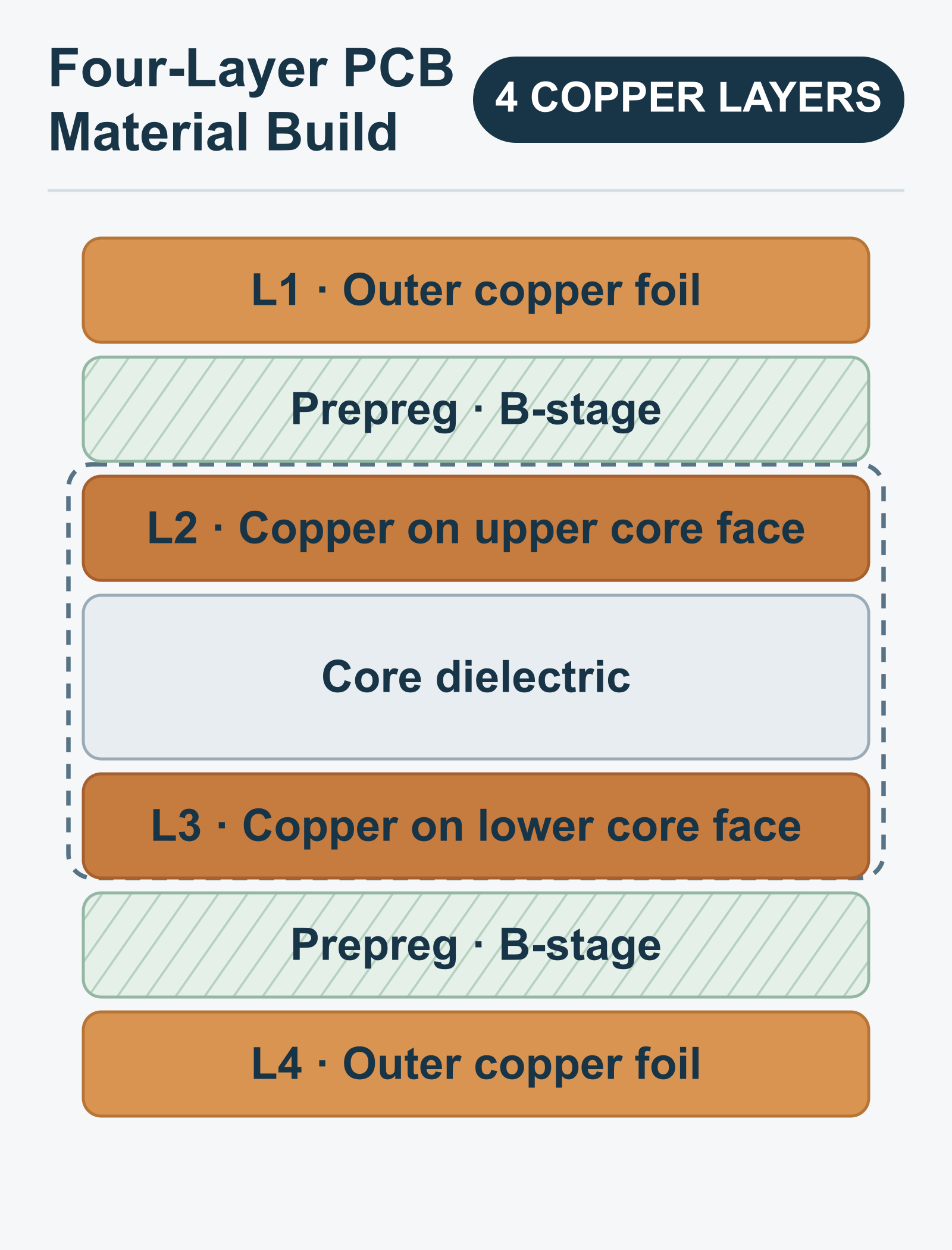
Figure 1. Simplified four-layer material build before lamination. Schematic, not to scale.
Material construction and layer function answer different questions. The material table records the core, prepreg, copper and finished board thickness. The layer assignment identifies signal, ground or power on L1 through L4. Keep both in one stackup revision so the design and fabrication teams can review the same build.
Via type is separate from layer count. A through-hole via can connect copper layers across the board, while blind and buried vias connect defined layer groups. State each via group’s start and end layers in the drill and stackup data. For the broader context, see the multilayer PCB stackup guide.
Read the sequence from L1 to L4, with S for signal, G for ground and P for power. In S/G/P/S, L1 signal traces sit beside L2 ground, while L4 traces sit beside L3 power. This assigns an inner layer to power distribution. A bottom-layer trace may use L3 as its reference when the copper under the trace is continuous and the power network is suitable for that signal.
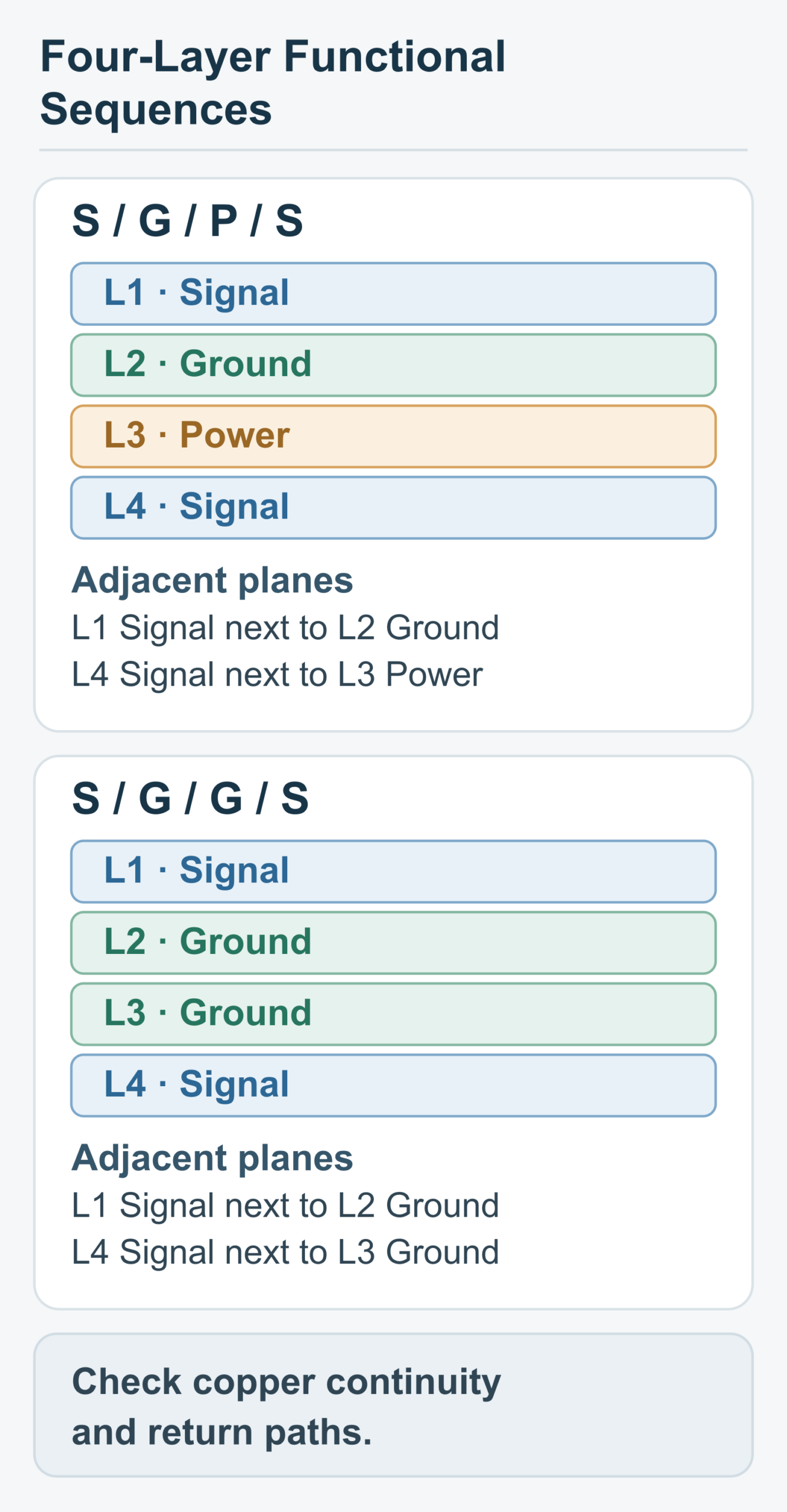
Figure 2. Two four-layer functional sequences and their adjacent inner planes. Schematic, not to scale.
A split in L3 can interrupt the reference beneath an L4 trace. Keep routes with fast edge rates over a solid power region when possible. If the layout cannot avoid a split, check the local return path and interface requirements. A lower edge-rate control signal may present less risk than a fast edge, but clock frequency alone does not describe edge rate.
In S/G/G/S, L1 and L4 sit beside L2 and L3 ground planes. Both outer signal layers therefore have an adjacent ground reference. Power traces or copper areas share the outer layers with signal routing, so compare the available space with the power demand before choosing this sequence.
Table 1 compares the two sequences by their outer-layer references, power distribution and routing checks. Use the function of each layer and the actual signal paths to decide whether either arrangement fits the design.
One anonymous four-layer project record lists a nominal finished board thickness of 1.0 mm with a tolerance of ±0.10 mm. It also lists a 0.7 mm core including copper and one 0.075 mm PP1080 layer on each side. These are the values in that one project record.
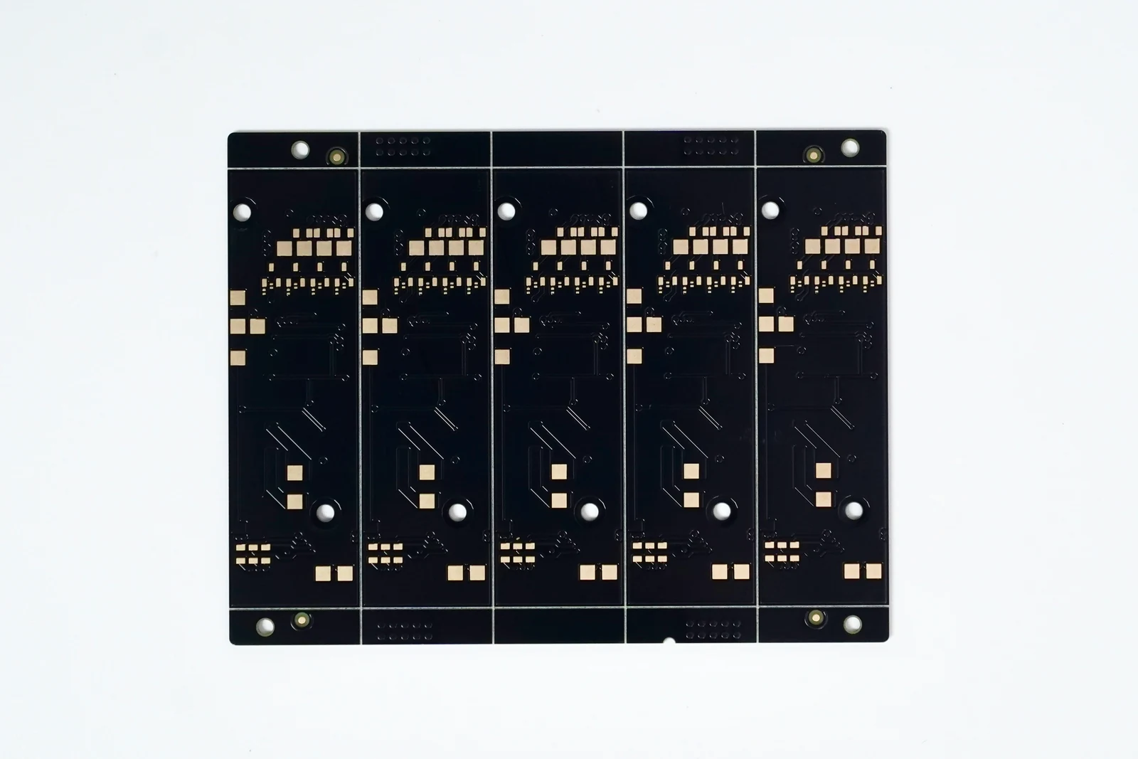
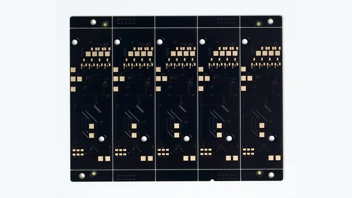
Figure 3. A black four-layer PCB panel with five repeated board sections.
Finished board thickness and trace-to-reference spacing are different measurements. For a top-layer trace that references L2, the local spacing runs from L1 to L2. For a bottom-layer trace that references L3, it runs from L4 to L3.
To confirm the prepreg thickness after lamination, use the material schedule and pressing data for the actual build. A sheet’s listed thickness alone does not give the final dielectric spacing.
For PCB impedance control, record the target and tolerance, signal and reference layers, trace width, copper thickness and dielectric properties. Add differential-pair spacing when it applies. If the material or pressed dielectric spacing changes, recalculate the cross-section and confirm any geometry change with the design owner.
Check the return path when a signal changes layers. In S/G/G/S, a top-to-bottom transition changes the adjacent reference from L2 ground to L3 ground. A ground stitching via near the signal via can connect those ground layers locally. Check for slots, clearances or dense via fields that interrupt the ground copper near the transition.
In S/G/P/S, the same transition moves from a ground reference to a power reference. A ground via connects ground layers, but it does not connect ground to power. If a power plane serves as the signal’s return reference, check its relationship to that signal and the high-frequency connection between power and ground.
The linked mixed-signal layout guidance covers designs with digital signals below 100 MHz and clock rise times above 1 ns. Within that scope, it considers the reference-plane transition and power-ground spacing used for decoupling. Evaluate the return connection at the edge rates and plane connections of the actual signal.
Use the four-layer comparison to identify the actual constraint. L3 power splits can interrupt the reference below critical L4 routes in S/G/P/S. In S/G/G/S, power traces or copper areas share outer-layer space with signal routes. Either constraint may justify evaluating a different layer count.
If the four-layer layout cannot fit the required signals and power while keeping suitable reference paths, state which conflict an added layer should solve. A higher layer count can provide more choices for signal, ground and power, but every critical layer change still needs a return path.
Compare fabrication quotes against the same material build, via spans, finished thickness and quantity. Layer count alone does not describe the work required to fabricate the board. For a different layer-count example, see the 6-layer PCB stackup guide.
Map the four copper files to L1 through L4 and list each layer’s function in the stackup table. Include the core, prepreg, copper and finished board requirements. Keep the layer files, drill data, board outline and fabrication notes on the same revision.
The drill data should distinguish plated and non-plated holes. For blind or buried vias, state the start and end layers for each group. If the design has controlled impedance, include its target, tolerance, signal and reference layers, and any permitted geometry adjustments in the pre-fabrication DFM review.
For multilayer bare PCBs, send the released layer and drill data, stackup, board outline and quantity. Include any special via or impedance requirements when you request a bare-board manufacturing quote from GemTech PCB.
S/G/G/S places L2 and L3 ground planes beside the L1 and L4 signal layers. Power uses traces or copper areas on the outer layers, so check that the available space can support both power and signal routing.
It can when the power copper is continuous beneath the trace and is suitable for that signal. If the route changes layers, also check the high-frequency connection between the power and ground references.
No. The project record lists the PP1080 sheet thickness, but the trace-to-plane spacing depends on the complete material build after lamination and on which layers the trace and reference use.
No. Add controlled-impedance requirements when the design calls for them. State the target, tolerance, trace and reference layers, and geometry needed for review.


