
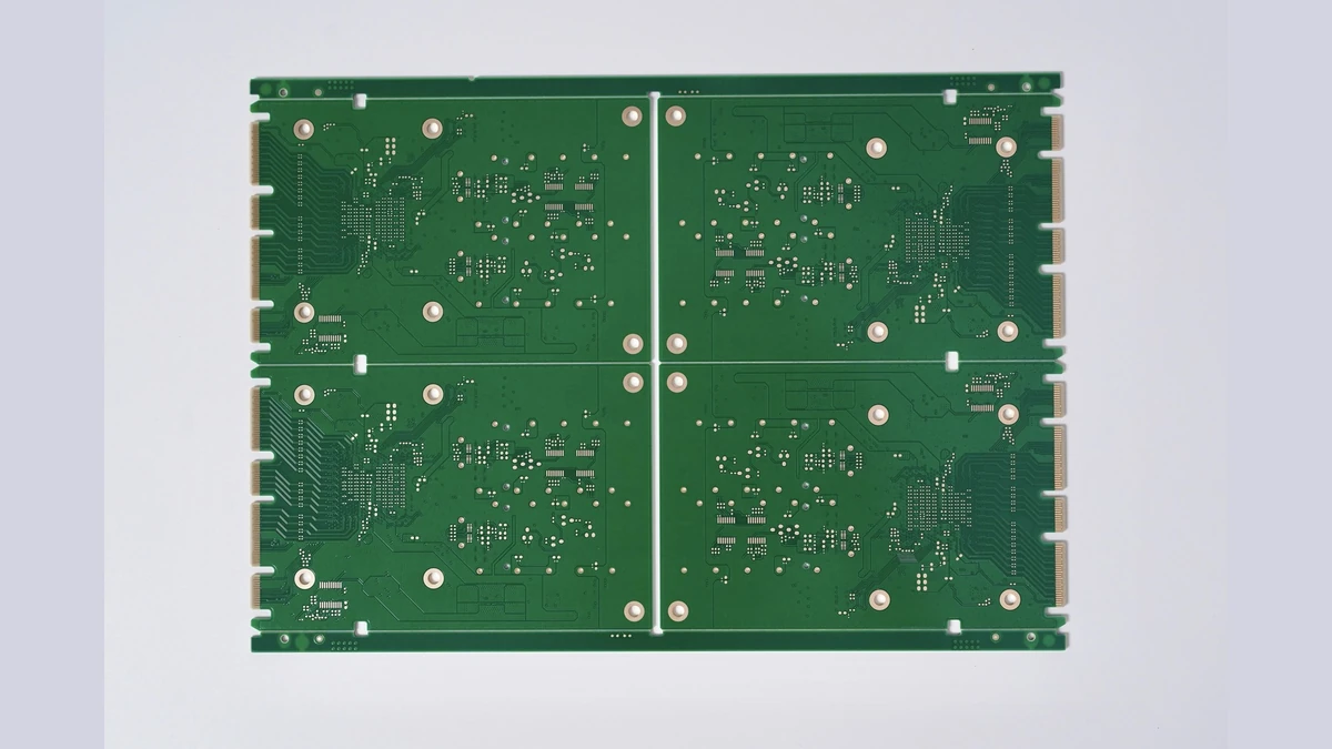
GEMTECH PCB
For an 8-layer PCB stackup, start by confirming which copper layer carries each critical net and which continuous reference copper lies nearby. Then compare the ground and power layer assignments, count core and prepreg (PP) positions and plies, and put the impedance structure and hole connection ranges in the same approved file set. The layer count alone does not identify actual net assignments, dielectric thickness, or impedance.
A reference plane is a continuous copper layer near a signal layer that can provide a return path. It is commonly a ground plane, but it can also be a power plane. Fast-changing signals develop a return path near an adjacent reference plane, so a stackup review should consider the signal routing layer, copper plane location, plane continuity, and net connections together.
If a signal crosses a plane split, the return path may detour and the loop area may increase. When a signal changes layers or its reference plane changes, confirm how the return path continues. Adjacency describes geometry only. It does not by itself show that a copper plane is suitable for a net.
List the routing layer, adjacent reference copper, and layer transition for each critical net before comparing stackups. If a ground or power plane is divided into several copper regions, check whether the net is assigned to a continuous, suitable region.
Altium’s high-speed PCB design article’s native 8-LAYER table lists Signal HS-H, GND, Signal HS-V, GND, POWER, Signal H, GND, and Signal V. Grouping signal layers as S, ground as G, and power as P gives S/G/S/G/P/S/G/S. The source also uses HS, H, and V labels for speed or routing direction. This sequence is an example from that table. Its reference relationships still depend on copper continuity and net assignment.
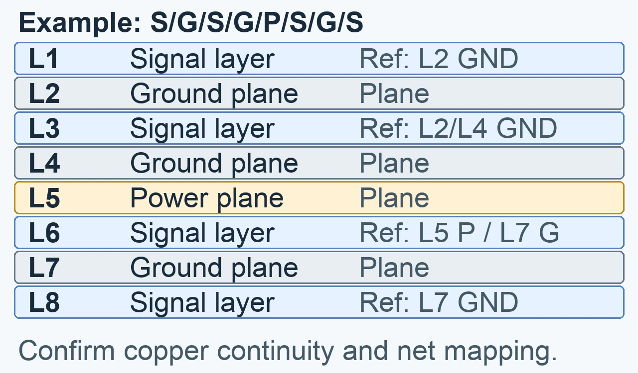
Figure 1. An S/G/S/G/P/S/G/S example with adjacent reference planes marked. Confirm the actual reference relationship from copper continuity and net assignment.
Another shorthand is S/G/S/P/P/S/G/S. Table 4-4 in TI’s AM62x LPDDR4 reference design labels L1 through L8 as TOP SIG/PWR, GND, SIG/PWR, PWR, PWR, SIG, GND, and BOTTOM SIG/PWR. L1, L3, and L8 have both signal and power functions, so S in the shorthand does not mean that a layer carries signals only. This layer order applies to the specified device reference board. Pages 4 to 5 of the guide and Table 4-4 stay within that application scope. See TI’s AM62x and AM62Lx DDR guide, pages 4 to 5 and Table 4-4.
The first example has three GND layers and one dedicated PWR layer. The TI example has two GND layers and two dedicated PWR layers, while also listing power nets on several SIG layers. Which arrangement applies depends on the nets, copper regions, and continuous reference paths. The local material record does not map signal, ground, or power functions to L1 through L8, so neither sequence identifies the project’s actual net assignment.
Eight layers means eight copper layers. Counting the spaces between adjacent copper layers gives seven dielectric gaps. Dielectric material type and ply count are separate records. They cannot be substituted for the copper layer count.
The local stackup record lists three core pieces and four PP positions across the seven gaps. Each PP position can contain one or more plies, so the number of PP plies can exceed the number of PP positions. This material example has three cores, four PP positions, and six PP plies in total.
An anonymized 8-layer material record specifies a nominal finished board thickness of 1.6 mm and FR-4 IT-180A. Each of the three cores is recorded as 0.13 mm, excluding copper. Two PP3313 positions each use one ply, recorded at 0.10 mm per ply. Two PP7628 positions each use two plies, recorded at 0.38 mm per two-ply group.
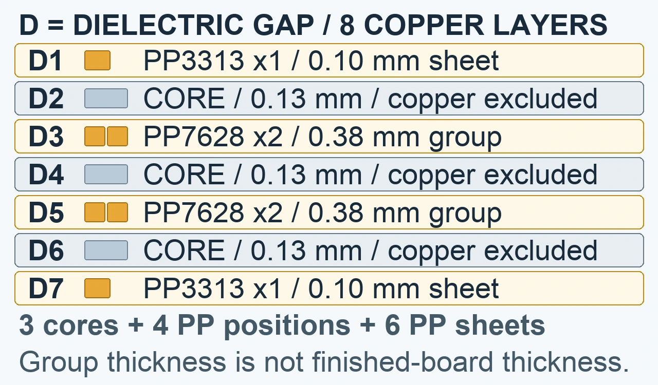
Figure 2. D marks a dielectric gap. The seven gaps, D1 to D7, follow the order in the anonymized material record.
For PP7628, 0.38 mm is the recorded thickness of a two-ply group, not one ply. The source does not state the single-ply thickness of those two PP plies, so it cannot be inferred from the combined value. The PP3313 value is recorded per ply. By ply count, the two PP3313 positions contain two plies and the two PP7628 positions contain four, for six PP plies in total.
Do not add these material labels to derive the 1.6 mm finished board thickness. Do not use one PP group thickness as the dielectric height for an impedance calculation. Finished thickness also depends on copper condition and material dimensions after lamination. Impedance spacing depends on the cross-section between the signal layer and its specified reference plane. Use the final approved product specification for finished-board thickness tolerance.
Impedance requirements must match the signal structure. For each single-ended or differential net, record the routing layer, reference layer, trace width, target impedance, and tolerance. For a differential net, also record the pair spacing. If the material or dielectric distance from the signal to its reference plane changes, the original trace width and spacing may no longer produce the same impedance. Use Altium’s impedance table fields and stackup confirmation notes when filling in the table. Keep these conditions together in the impedance table and stackup drawing.
A stackup change alters the dielectric and reference conductor positions around a signal. Recheck the trace width, differential pair spacing, and target value for the affected nets against the final cross-section. Before fabrication, match the impedance table approved by the design team to the approved material structure. Do not transfer an impedance value from a reference design to another 8-layer board as a general requirement.
Identify plated through holes (PTHs), blind vias, and buried vias by hole type and connection range. Blind and buried vias also need their start and end layers. Identify non-plated through holes (NPTHs) separately. Their walls do not provide plated interlayer connections. Match hole type, start and end layers, layer order, and plating notes across the files. The eight-layer count alone does not determine hole structure or manufacturing process.
Keep the layer order, material, impedance, and drill files on the same revision. If versions differ in thickness tolerance or material substitution, identify the version that needs approval before requesting a quote. Use this checklist:
For the full relationship between materials and layer count, see the multi-layer PCB stackup guide. For other layer counts, compare the four-layer PCB stackup and six-layer PCB stackup articles. Review the product scope on the multi-layer bare-board manufacturing page, then submit the files through the bare-board manufacturing quote section.
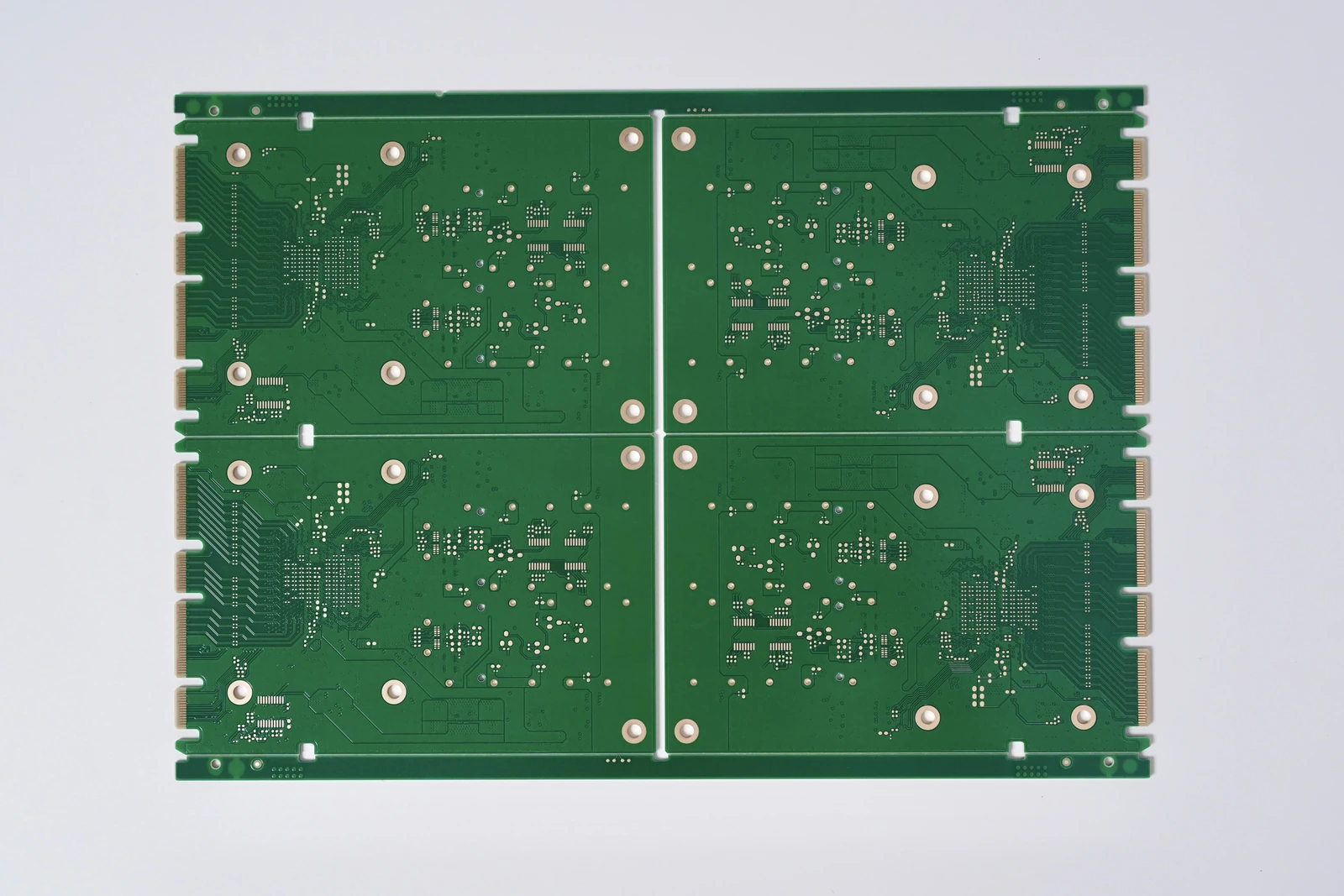
Photograph of a green PCB panel from another project.


