

Choose a PCB surface finish based on the purpose of each exposed copper area. Component pads need solderability and planarity, and the finish must fit the assembly process. Edge-connector contacts and wiping contacts also need to account for contact wear. If a board has both solder pads and contacts that plug into a connector, the fabrication data should identify the finish and boundary for each area. Terms such as "gold finish," "lead-free," or "standard finish" do not specify the process used on each area.
This guide compares hot air solder leveling (HASL), electroless nickel immersion gold (ENIG), organic solderability preservative (OSP), immersion tin, immersion silver, and hard gold. It explains how to record the areas, solder-mask openings, via fill, and assembly conditions in the same fabrication package. The designer and current fabricator should confirm the available finishes and acceptance requirements for each job.
Surface finishes protect exposed copper at solder-mask openings and provide a surface for soldering or electrical contact. Solder pads need to meet solderability and assembly requirements; edge-connector contacts also experience insertion or wiping. The two areas serve different purposes, so color alone cannot determine the process.
Gold fingers are contact areas along a board edge, typically used with an edge connector or wiping contact. Contact method, insertion frequency, and wear affect finish requirements, so check the mating connector's requirements for insertion and contact wear.
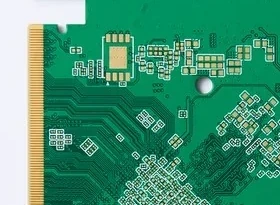
Figure 1. Close-up of the edge contact strip and adjacent pads.
ENIG and electroplated gold over nickel use different process structures. ENIG deposits electroless nickel on the copper and then immersion gold. For hard gold in designated contact areas, state the finish and mark its location on the drawing rather than writing only "gold finish".
Color describes appearance, but it cannot identify the layer structure, plating type, or selective coverage area. If the gold or nickel layers, insertion area, or appearance have acceptance requirements, state them in the same drawing or process specification revision.

Figure 2. Solder pads, edge contacts, and simplified ENIG and hard-gold structures. Layer thicknesses are not to scale.
Use the following sequence to complete the application details before comparing finishes.
Surface finish is part of PCB outer-layer manufacturing. To see where it sits in the process, read the multilayer PCB manufacturing process.
The table compares surface structures, common uses, and items to verify. Check fine-pitch pads, connector contacts, and storage conditions against the actual assembly requirements.
Review HASL pad-height variation, OSP sensitivity to handling and contamination, and possible discoloration of exposed immersion silver against the assembly and storage conditions. Use the current process specification to set packaging, storage after opening, and assembly conditions.
Surface finish covers the exposed areas specified in the fabrication data. The solder-mask layer should identify openings and contact areas to remain exposed. Their boundaries should align with the copper artwork, board outline, and connector insertion direction.
For via-in-pad or resin-filled vias near a pad, the drill and via-fill files should state whether the hole is left open, filled, or capped with copper. Then confirm that the via treatment is compatible with the selected surface finish. Do not specify ENIG in the finish field while omitting via requirements.
If the laminate, stackup, finished-board thickness, or assembly thermal process has special requirements, submit the stackup, solder-mask, via-treatment, and assembly files at the same revision. This lets the fabricator and assembler check them against the actual process. Surface finish names do not replace material or assembly conditions.
One anonymized project specifies gold plating for edge contacts and immersion gold. The drawing still needs to show the area, boundary, and acceptance criteria for each requirement. Listing finish names alone does not show where they apply.
If the via-fill, solder-mask, and surface-finish notes use different revisions, first identify the revision that is in effect. For file alignment and engineering approval before manufacturing, see PCB DFM review before manufacturing.
When submitting bare-board fabrication data, include at least these three items:
For the layer and material context, read our multilayer PCB stackup guide.
After confirming the board construction and bare-board manufacturing requirements, see our PCB manufacturing page for manufacturing information and submit a quote request with the surface finish requirements.


