

GEMTECH PCB
A multilayer PCB manufacturing process typically starts with approved production data, then moves through inner-layer circuitry, lamination, drilling and hole-wall metallization, outer-layer patterning, solder mask and surface finish, and finally bare-board inspection and profiling. The exact route depends on the stack-up, hole types, and surface-finish requirements.
The process below follows a common multilayer bare-board route with mechanically drilled through-holes. It explains what each stage processes, what it produces, and what to check. Blind vias, buried vias, and sequential lamination change some of the steps.
The table summarizes a common multilayer bare-board route with mechanically drilled through-holes, from engineering data through bare-board inspection. It lists each stage’s process, output, and checks. The exact sequence varies with the stack-up, hole types, and surface-finish requirements.
Both stages turn a copper surface into a circuit pattern, but the protected areas after imaging and the order of copper removal differ.
Here is one common inner-layer route using negative dry film:
The inner-layer image can be checked against the approved data for that layer. If another photoresist material is used, confirm which areas remain according to its imaging rules and the photoplot data.
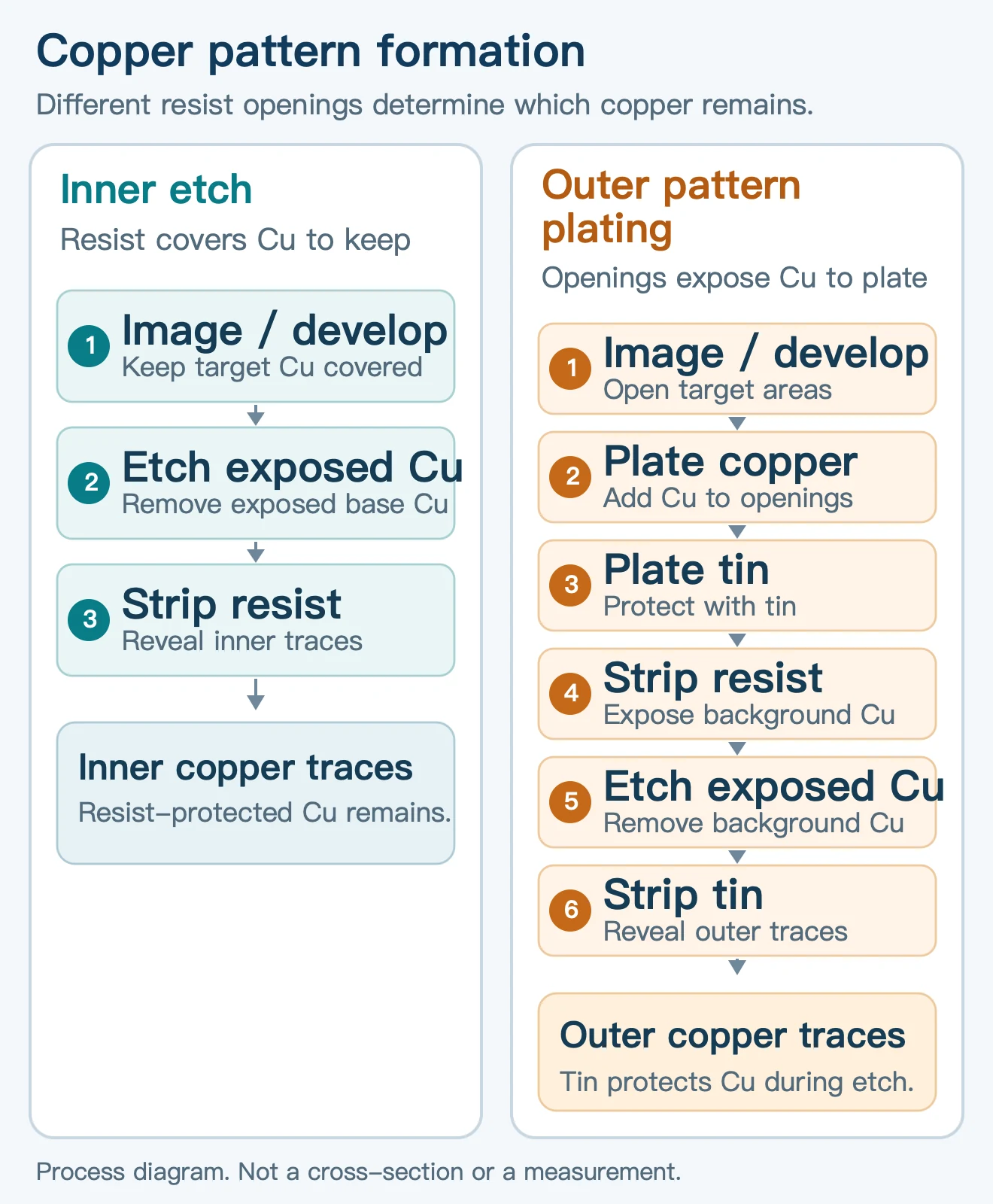
Figure 1. Protected areas and removal order in inner-layer etching and outer-layer pattern plating.
Figure 2 shows the developing-line equipment and process sign on site.
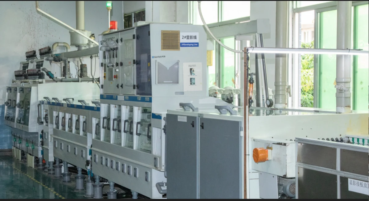
Figure 2. Developing-line equipment and its process sign.
One example is a pattern-plating route that uses tin as the etch resist:
Resist stripping, etching, and tin stripping act on different materials.
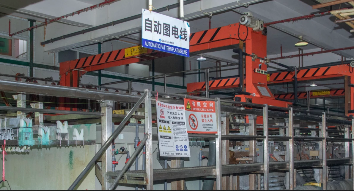
Figure 3. Automatic pattern-plating equipment and its process sign.
Align the inner-layer cores, prepreg, and outer-layer copper foil, then stack them according to the approved stack-up. During lamination, the prepreg resin flows and cures under heat, bonding adjacent materials into a board. Material type, stack order, and engineering requirements determine the specific lamination plan.
To read a board’s layer structure, start with the multilayer PCB stack-up guide, then review the 4-layer PCB stackup, 6-layer PCB stackup, or 8-layer PCB stackup example that matches the layer count. These explain layer names, material positions, and layer relationships. They do not replace the project’s approved stack-up table.
A common mechanically drilled multilayer board is drilled for through-holes after lamination. The drill table must also distinguish plated and non-plated holes. Blind and buried vias have different start and end layers from a standard through-hole and may require sequential lamination or another process sequence. The hole type and layer-connection range must be matched item by item in the production data.
Figure 4 shows mechanical drilling equipment and the board-processing area.
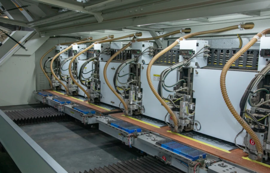
Figure 4. Mechanical drilling equipment and the board-processing area.
After drilling, clean the hole walls and remove resin residue. Resin and glass fiber are not conductive, so holes that need copper plating first receive a conductive layer. Copper is then built up on the hole wall by electroplating. Electroless copper deposition and direct metallization are different methods for creating this conductive layer. The selected method and pretreatment conditions depend on the actual process.
Whether a copper pad is retained beside the hole is determined by the copper-layer pattern and connection design.
If an NPTH is drilled before the relevant plating stage, the process must keep copper out of the hole. The hole may also be drilled after plating.
Figure 5 compares a copper-plated PTH wall with an unplated NPTH wall. Confirm the actual hole type against the drill table, copper-layer patterns, and fabrication notes.
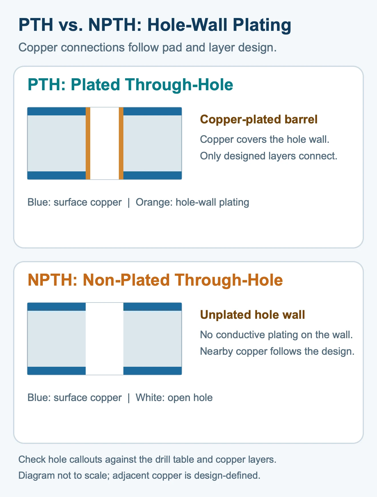
Figure 5. Illustration of the hole-wall metallization difference between PTH and NPTH. The copper pattern beside each hole follows the design data, and the drawing is not to scale.
After outer-layer copper patterning, solder mask covers areas that do not need soldering and exposes pads and specified locations according to the opening data. Exposed copper then receives the surface finish required for the project. Legend text identifies reference designators, polarity, and other features. The exact order of solder mask, surface finishing, and legend printing depends on the selected process and should be checked against the approved data.
Automated optical inspection (AOI) compares the copper pattern with the corresponding layer data.
A bare-board electrical test uses the netlist, which lists electrical connections, and the approved board data to check continuity and isolation. It checks electrical connections on the bare board. It does not verify the assembled product’s function. The test objects and required coverage must come from the project data.
The order of bare-board electrical testing and profiling follows the approved production flow. Profiling machines the board outline, slots, and panelization features.
After profiling, final inspection checks the specified outline, holes, and board-surface items against the mechanical drawing and finished-board requirements.
Production records should list the inspected objects and results separately for pattern inspection, bare-board electrical testing, and finished-board visual and mechanical inspection.
The production data should specify these fields:
If layer names, hole types, or revisions conflict across the files, confirm them before generating production data.
Together, the production data determines the inner- and outer-layer patterns, lamination, drilling, hole-wall metallization, and inspection plan. Stating the actual hole types and layer connections helps the fabricator verify the route more than layer count alone. Before production, use the PCB DFM review checklist to align these requirements.
For an overview of bare-board fabrication, see the multilayer bare-board fabrication page. To have specific engineering files reviewed, submit them through the bare-board fabrication quote form.


